
Page 535 - DSP Integrated Circuits
P. 535
520 Chapter 11 Processing Elements
11.19.2 Control PEs
It is possible to implement the loop counters i and k with an 8-bit counter [29]. The
indices of x(i) can be interpreted as addresses in memories which can be extracted
from this counter. For the coefficients, WP, we need the exponent p. Notice that W
= exp(27y'/AO and hence the binary representation of p can be interpreted as a& as
just discussed. It is also possible to extract p from the same 8-bit counter [29].
A drawback of implementing the control units using a bit-serial style is the
high clock frequency that is required. It may therefore be better to use a bit-paral-
lel or digit-serial implementation to reduce the required clock frequency and possi-
bly also the power consumption.
11.19.3 Address PEs
Control of the architecture is captured in the address processors for the RAMs. A behav-
ioral description of the address processors was derived in Section 9.9. The base index
generator has three modes of operation: input, FFT computation, and output. During
the input and output phases it must compute the data index, i, and which RAM this
data belongs to. The index is in the interval 0 < i < 1024. During the FFT computation,
the base index generator computes m, k\, and the Gray code equivalent of k\.
During the input and output phases, index i can be almost directly used as an
address to the RAMs. The exception is that the index must be bit-reversed during
the output phase and must be truncated to 9 bits. Hence, the function of the
address generators for the RAMs is trivial.
During the FFT computation, index m must be extended to become an
address. The location of the extra bits is controlled by the Stage. The positions of
these bits have the same weight as N s and BF:
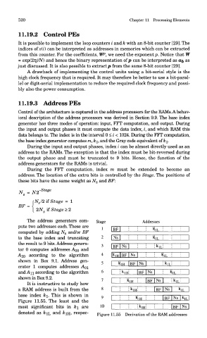
Stage
N s = N2~
\N s/2 if Stage = 1
BF =
2N sifStage>2
The address generators com- Stage Addresses
pute two addresses each. These are 1 BF k
computed by adding N s and/or BF ML I
to the base index and truncating Ns k ML :
the result to 9 bits. Address genera- BF Ns kiLi
tor 0 computes addresses AQQ and
A10 according to the algorithm |k m BF Ns HlL
shown in Box 9.1. Address gen- BF Ns
erator 1 computes addresses AQI * 1H ikiL
and AH according to the algorithm k 1H BF Ns i kj 1L
shown in Box 9.2.
k 1H BF Ns | klL
It is instructive to study how
a RAM address is built from the k lH BF|Ns n 1L
base index k\. This is shown in
k
Figure 11.55. The least and the rlH |BF Ns k, L
most significant bits in k\ are 10 k lH i BF Ns
denoted as &IL and &IH, respec- Figure 11.55 Derivation of the RAM addresses