
Page 297 - Engineering Digital Design
P. 297
268 CHAPTER 6 / NONARITHMETIC COMBINATIONAL LOGIC DEVICES
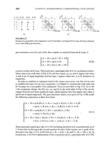
A B A>B A=B A<B
0 0 gt eq It
0 1 0 0 1
1 0 1 0 0
1 1 gt eq It I ^2! ^alx
X(A>B)
FIGURE 6.27
Design of a cascadable 1-bit comparator, (a) EV truth table, (b) Output EV K-maps showing minimum
cover with XOR-type functions.
gate-minimum cover for each of the three outputs, as extracted from the K-maps, is
(A > B) = gt(AOB) + AB
(A = B) = eq(AOB) (6.20)
(A < B) = lt(A QB) + AB
as given in three-level form. These represent a gate/input tally of 8/16, excluding inverters.
Notice that in the truth table of Fig. 6.27a all three inputs, gt, eq, and It, appear only when
A and B are of equal magnitude and that logic 1 appears when one, A or B, dominates in
magnitude.
In order to establish an important trend in the output expressions, one that can be used
to establish the logic for any size comparator, it is helpful to construct the truth table and
EV K-maps for a cascadable 2-bit comparator. These are provided in Fig. 6.28. As in the
1-bit comparator design, the EVs (gt, eq, and If) in the truth table of Fig. 6.28a are the
outputs from the next least significant stage, which explains why they appear only when A
and B are of equal magnitude. The gate-minimum output cover given in Fig. 6.28b yields
the following expressions in three-level form:
(A > B)
= gt(A { O Bi)(A 0 O BQ) + A 0B 0(A ] O
(A = B) = eqA 0Bo(A 1 O B {) + eqA 0B 0(A l Q B
(6.21)
(A < B) = A 0(lt+B 0)(A l O 50 + ltA 0B 0(A l
O B {)(A 0 O B 0) + Aoflo(Ai O
These represent a gate/input tally of 1 1/29 (excluding inverters) with a maximum fan-in of
4. Notice that in arriving at the second equation for each of the outputs, use is made of the
absorptive law, Eqs. (3.13), in the form gt+ B 0 = gtB 0 + BQ and It + B 0 = ltB 0 + B Q. In
comparison, a two-level optimization of this comparator gives a gate/input tally of 21/60,