
Page 298 - Engineering Digital Design
P. 298
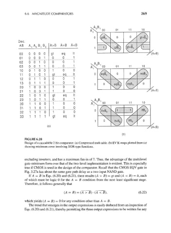
6.6 MAGNITUDE COMPARATORS                                            269


             Dec.
             AB    A. A 0 B. B n  A>B  A-B  A<B
                            0
             00   0  0  0 0    gt     eq    It                                            (A>B)
             01   0  0  0 1     0     0     1
             02   0  0 1 0      0     0     1
             03   0  0 1 1      0     0     1         AX     00      01      11     10
             10   0  1  0  0    1     0     0           1
             11   0  1  0 1     gt    eq    It              feqB,                  eqB c
             12   0  1 1   0    0     0     1
             13   0  1 1 1      0     0     1
             20    1  0 0 0     1     0     0                       eqB c   eqB c        /
             21    1  0 0 1     1     0     0                                             (A=B)
             22   1 0 1 0       gt    eq    It
             23   1  0 1 1      0     0     1           A  B
             30   1 1 0 0       1     0     0          \  0 1  °0    01      11 10
             31   1 1 0 1       1     0     0              /"N           .   ...  /"\
             32   1 1 1 0       1     0     0           0  (lt+B,  \ll —  — y/      "Bo)
             33   1 1 1    1    gt    eq    It
                                                              0\           <*y /„
                                                                  s^i)


                                                                        (b)
                 FIGURE 6.28
                 Design of a cascadable 2-bit comparator, (a) Compressed truth table, (b) EV K-maps plotted from (a)
                 showing minimum cover involving XOR-type functions.


                 excluding inverters, and has a maximum fan-in of 7. Thus, the advantage of the multilevel
                 gate-minimum form over that of the two-level implementation is evident. This is especially
                 true if CMOS is used in the design of the comparator. Recall that the CMOS EQV gate in
                 Fig. 3.27a has about the same gate path delay as a two-input NAND gate.
                    If A = B in Eqs. (6.20) and (6.21), there results (A > B) = gt and (A < B) = It, each
                 of which must be logic 0 for the A = B condition from the next least significant stage.
                 Therefore, it follows generally that


                                        (A = B) = (A > B) • (A < B),                (6.22)

                 which yields (A = B) = 0 for any condition other than A = B.
                   The trend that emerges in the output expressions is easily deduced from an inspection of
                 Eqs. (6.20) and (6.21), thereby permitting the three output expressions to be written for any