
Page 384 - Engineering Digital Design
P. 384
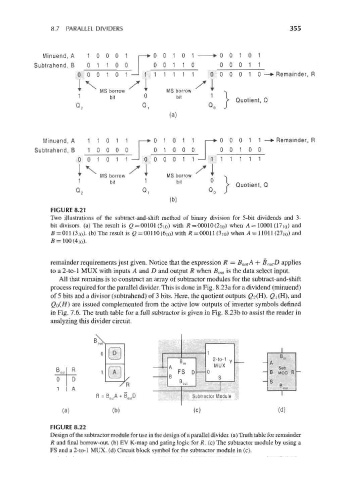
8.7 PARALLEL DIVIDERS                                               355


                Minuend, A 1000 1          .—> 0010 1           >> 0010 1
             Subtrahend, B 0110 0              0011 0             0001 1
                          000101—'11111 1                      00001 0 —*> Remainder, R
                          IN            xi
                          T
                                MS borrow   T      MS borrow
                          1        bit                bit
                                             °                  •   } Quotient, Q
                                            Q,                 ~
                         Q 2
                                                    (a)


                Minuend, A 1101 1              0101 1         |—> 000 1 1 —> Remainder, R
             Subtrahend, B 1000 0              0100 0              0010 0
                          00 1 0 1 1—1 000011—111111 1
                          iv
                          T
                                MS borrow   T      MS borrow
                          1        bit      1        bit
                                                               -   >> Quotient, Q
                                            Q,                 -
                         Q 2
                                                    (b)
                  FIGURE 8.21
                  Two illustrations of the subtract-and-shift method of binary division for 5-bit dividends and 3-
                  bit divisors, (a) The result is Q =00101 (5io) with R =00010(2 ]0) when A = 10001 (17i 0) and
                  B = 011 (3i 0). (b) The result is Q =00110(6 10) with R = 00011 (3i 0) when A = 11011 (2?i 0) and
                  fl = 100(4i 0).


                  remainder requirements just given. Notice that the expression R = B OU,A + B OU,D applies
                  to a 2-to-l MUX with inputs A and D and output R when B out is the data select input.
                    All that remains is to construct an array of subtracter modules for the subtract-and-shift
                  process required for the parallel divider. This is done in Fig. 8.23a for a dividend (minuend)
                  of 5 bits and a divisor (subtrahend) of 3 bits. Here, the quotient outputs £2(H), Q \ (H), and
                  <2o(#) are issued complemented from the active low outputs of inverter symbols defined
                  in Fig. 7.6. The truth table for a full subtracter is given in Fig. 8.23b to assist the reader in
                  analyzing this divider circuit.


                       D
                       A              _               t
                                                          Subtracter Module
                                                          (C)
                  FIGURE 8.22
                  Design of the subtractor module for use in the design of a parallel divider, (a) Truth table for remainder
                  R and final borrow-out, (b) EV K-map and gating logic for R. (c) The subtractor module by using a
                  FS and a 2-to-l MUX. (d) Circuit block symbol for the subtractor module in (c).