
Page 389 - Engineering Digital Design
P. 389
360 CHAPTER 8 / ARITHMETIC DEVICES AND ARITHMETIC LOGIC UNITS (ALUs)
ii M, S,, S n
' °
M(H) B A
C ln(H)
1-bit c
ALU tn
A(H)
S 0(H) _
r
C 011,(H)
(b)
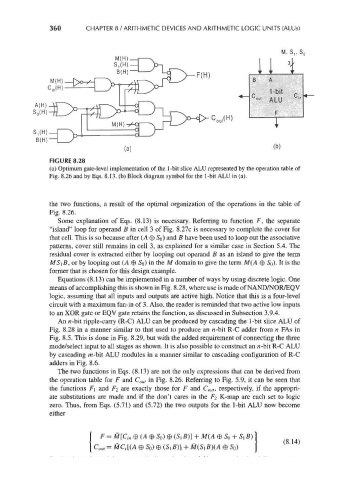
FIGURE 8.28
(a) Optimum gate-level implementation of the 1-bit slice ALU represented by the operation table of
Fig. 8.26 and by Eqs. 8.13. (b) Block diagram symbol for the 1-bit ALU in (a).
the two functions, a result of the optimal organization of the operations in the table of
Fig. 8.26.
Some explanation of Eqs. (8.13) is necessary. Referring to function F, the separate
"island" loop for operand B in cell 3 of Fig. 8.27c is necessary to complete the cover for
that cell. This is so because after (A 0 So) and B have been used to loop out the associative
patterns, cover still remains in cell 3, as explained for a similar case in Section 5.4. The
residual cover is extracted either by looping out operand B as an island to give the term
MS\ B, or by looping out (A 0 So) in the M domain to give the term M(A 0 So). It is the
former that is chosen for this design example.
Equations (8.13) can be implemented in a number of ways by using discrete logic. One
means of accomplishing this is shown in Fig. 8.28, where use is made of NAND/NOR/EQV
logic, assuming that all inputs and outputs are active high. Notice that this is a four-level
circuit with a maximum fan-in of 3. Also, the reader is reminded that two active low inputs
to an XOR gate or EQV gate retains the function, as discussed in Subsection 3.9.4.
An n-bit ripple-carry (R-C) ALU can be produced by cascading the 1-bit slice ALU of
Fig. 8.28 in a manner similar to that used to produce an n-bit R-C adder from n FAs in
Fig. 8.5. This is done in Fig. 8.29, but with the added requirement of connecting the three
mode/select input to all stages as shown. It is also possible to construct an n-bit R-C ALU
by cascading w-bit ALU modules in a manner similar to cascading configuration of R-C
adders in Fig. 8.6.
The two functions in Eqs. (8.13) are not the only expressions that can be derived from
the operation table for F and C out in Fig. 8.26. Referring to Fig. 5.9, it can be seen that
the functions F\ and F^ are exactly those for F and C out, respectively, if the appropri-
ate substitutions are made and if the don't cares in the FZ K-map are each set to logic
zero. Thus, from Eqs. (5.71) and (5.72) the two outputs for the 1-bit ALU now become
either
F = M[C in © (A 0 So) 0 (5, B)] + M(A 0 S 0 + S, B) j
C oul = Md [(A 0 S 0) 0 (S, B)] + M(Si B)(A 0 S 0) I