
Page 393 - Engineering Digital Design
P. 393
364 CHAPTER 8 / ARITHMETIC DEVICES AND ARITHMETIC LOGIC UNITS (ALUs)
Cin(L)
Cin(L)-^-i p«-C in(L]
1 1
C r rt m Ij-l cto/io 11 From J-1 stage
From J+1 stage
Cri
I I
D 3-D 0(H)
i EN(L)
3 2 1 0 I A
EN
J* Y *\ S Y — F(H)
M(L)-C EN — ^ 1 J m
MUX-D Y
MUX-R
s, s fl P(L) i — \ n ^ >>-| S 0 Y O-F(L)
i ' 321 0
A(H) — ^
th
J AOI Gate t'
B(H)
s, s 0 R 3-R 0(H)
E(H)
jm Y
J(L)-C EN
MUX-E Y 0- (3
EN
3 2 1 0
Ith
L/R(H) - DMUX
0 1
E 3-E 0(H)
C out(L)<«— I L- -*C out(L)
To J+1 stage To J-1 stage
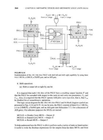
FIGURE 8.34
Implementation of the 7th 1-bit slice PALU with shift left and shift right capability by using three
4-to-l MUXs, a DMUX, a NAND gate, and an AOI gate.
4. Shift operations
(a) Shift or rotate left or right by one bit
It is required that each 1-bit slice of the PALU have a resulting output function F and
that the PALU be cascaded with respect to the carry-in and carry-out parameters, C in and
C out. Also, it is required that the PALU operate with/a/se carry rejection, that is, that C OM
be disabled for all nonarithmetic operations.
The logic circuit diagram for the Jth 1-bit slice PALU and its block diagram symbol are
presented in Figs. 8.34 and 8.35. As can be seen, the PALU consists of three 4-to-l MUXs,
a l-to-2 DMUX, a NAND gate, and an AOI gate (see Subsection 7.7.1 for a discussion of
AOI gates). For reference purposes the MUXs are named
MUX-D => Disable Carry MUX — Output D
MUX-E => Extend Carry MUX — Output E
MUX-R => Result MUX — Output F
To help understand how the PALU is able to perform such a variety of tasks as listed earlier,
it useful to write the Boolean expressions for the outputs from the three MUXs and from