
Page 394 - Engineering Digital Design
P. 394
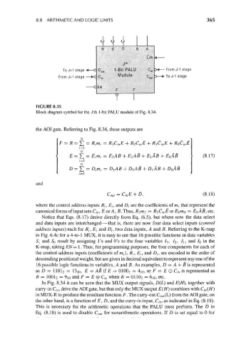
8.8 ARITHMETIC AND LOGIC UNITS                                      365


                                            4   4 4

                                            R    E  D     B   A

                                                              Dft «—
                             To J+1 stage « C  C OUl  1-Bit PALU  c !n  >« — From J-1 stage
                                                   Mudule
                           From J+1 stage — XI c iB               3 — > To J-1 stage
                                                              ^Oul
                                         c EN
                                                  F      F
                                                 T

                  FIGURE 8.35
                  Block diagram symbol for the 7th 1-bit PALU module of Fig. 8.34.


                  the AOI gate. Referring to Fig. 8.34, these outputs are
                                    o
                           F = R = £ = Ritrii = R^CinE + R 2C inE + RiC inE + R 0C inE
                                   (=3
                                    0
                               E = Y< = EM = EiAB + E 2AB + E {AB + E 0AB            (8.17)
                                   i=3
                                    0
                               D = ]T = D,m/ = D 3AB + D 2AB + D]AB + D QAB
                                   i=3

                  and
                                              C out = C,nE + D,                      (8.18)

                  where the control address inputs /?/, £,-, and D,- are the coefficients of m, that represent the
                  canonical forms of input sets C in, E or A, B. Thus, R 2 m 2 = R 2Ci nE or EQWQ = EoAB, etc.
                    Notice that Eqs. (8.17) derive directly from Eq. (6.5), but where now the data select
                  and data inputs are interchanged—that is, there are now four data select inputs (control
                  address inputs) each for /?/, E, and D/, two data inputs, A and B. Referring to the K-map
                  in Fig. 6.4c for a 4-to-l MUX, it is easy to see that 16 possible functions in data variables
                  S\ and SQ result by assigning 1's and O's to the four variables IT,, I 2, I\, and /o in the
                  K-map, taking EN= 1. Thus, for programming purposes, the four components for each of
                  the control address inputs (coefficients of m,), /?,-, £/, and D,, are encoded in the order of
                  descending positional weight, but are given in decimal equivalent to represent any one of the
                  16 possible logic functions in variables, A and B. As examples, D = A + B is represented
                  as D = 1101 2 = 13io, E = AB if E = 0100 2 = 4 10, or F = E O C in is represented as
                  R = 1001 2 = 9io and F = E © C in when R = 0110 2 = 610, etc.
                    In Fig. 8.34 it can be seen that the MUX output signals, D(L) and E(H), together with
                  carry-in C- m, drive the AOI gate, but that only the MUX output E(H) combines with Ci n(H)
                  in MUX-R to produce the resultant function F. The carry-out C out(L) from the AOI gate, on
                  the other hand, is a function of E, D, and the carry-in input, C, n, as indicated in Eq. (8.18).
                  This is necessary for the arithmetic operations that the PALU must perform. The D in
                  Eq. (8.18) is used to disable C out for nonarithmetic operations. If D is set equal to 0 for