
Page 391 - Engineering Digital Design
P. 391
362 CHAPTER 8 / ARITHMETIC DEVICES AND ARITHMETIC LOGIC UNITS (ALUs)
S
\ 1
MV 0 1 MV 0 1
0 (A©S O A©s 0 ]e[ij 0 © (B(AeSo)]
1 0 0 1 0 0
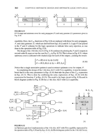
FIGURE 8.31
EV K-maps and minimum cover for carry propagate (P) and carry generate (G) parameters given in
Fig. 8.30.
capability. Here, the C ou[ functions of Fig. 8.26 are replaced with those for carry propagate,
P, and carry generate, G, which are derived from Eqs. (8.2) and (8.7). Logic O's are placed
in the P and G columns for the logic operations to indicate false carry rejection, as was
done in the operation table of Fig. 8.26.
The design of the 1-bit slice ALU of Fig. 8.30 continues by plotting the P and G outputs in
second-order K-maps as was the case for C out in Fig. 8.27d. This is done in Fig. 8.31, where
optimum cover is indicated with shaded loops for each of the outputs, yielding the results
_ — > . (8.16)
G = M(S 1B}(A 0 S 0) + MSiS 0A J
Notice that a single associative pattern is used to extract optimum cover for output, P.
In completing the design of the 1-bit slice ALU with CLA capability, it must be remem-
bered that it is the carry parameters in Eqs. (8.16) that take the place of the C ou, expression
in Eqs. (8.13). This is done by combining the carry expressions of Eqs. (8.16) with the
expression for function F in Eqs. (8.13). The result is the logic circuit in Fig. 8.32a and its
block diagram symbol in Fig. 8.32b for a 1-bit slice ALU with CLA capability.
M(H).
S^H) —
B(H)—I ' LdpN Rm M,S 1 ,S D
( }
M(H)_bo^| V ,\r-^ PLX - |
B
1 -bit CLA
ALU
FIGURE 8.32
(a) Optimum gate-level implementation of the 1-bit slice ALU with CLA capability represented by
the operation table of Fig. 8.30 and by Eqs. (8.16). (b) Block diagram symbol for the 1-bit ALU in (a).