
Page 388 - Engineering Digital Design
P. 388
8.8 ARITHMETIC AND LOGIC UNITS 359
the three mode/select inputs M, S\, and SQ. On the right side of the table are the function
expressions F, a brief description of each function operation, and carry-out expressions,
C ou!. The expressions for F and C (mt are deduced from Eqs. (8.2) for the full adder (FA)
together with Eqs. (3.23). Note that false carry rejection during the logic mode is realized
by placing zeros in the C out column for the four logic operations — the carry-out function
has no relevance in a logic operation. Notice further that the two possible logic states for
Ci n lead to different interpretations for each of the four arithmetic operations. For example,
A © Ci n is the transfer of A if C- m = 0, but represents the increment of A if the LSB C in = 1
(B = 0 is implied). Or, A © Cm represents the 1's complement of A if LSB C in = 0 but is
the 2's complement of A if LSB C- m = 1 (B = 1 is implied). Subtraction operations by this
ALU are carried out by 2's complement arithmetic as discussed in Subsection 2.9.2.
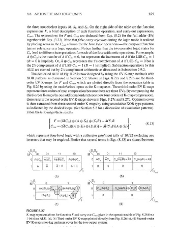
The dedicated ALU of Fig. 8.26 is now designed by using the EV K-map methods with
XOR patterns as discussed in Section 5.2. Shown in Figs. 8.27a and 8.27b are the third-
order EV K-maps for F and C out, which are plotted directly from the operation table in
Fig. 8.26 by using the mode/select inputs as the K-map axes. These third-order EV K-maps
represent three orders of map compression because there are three EVs. By compressing the
third-order K-maps by one additional order (hence now four orders of K-map compression),
there results the second-order EV K-maps shown in Figs. 8.27c and 8.27d. Optimum cover
is then extracted from these second-order K-maps by using associative XOR-type patterns,
as indicated by the shaded loops. (See Section 5.2 for a discussion of associative patterns).
From these K-maps there results
}, (o.lj)
C out = (MC ln)[(A © So) © (S, B)] + M(Si B)(A © S 0) J
which represent four-level logic with a collective gate/input tally of 10/22 excluding any
inverters that may be required. Notice that several terms in Eqs. (8.13) are shared between
M\ 00 01 11 10 M\ 00 01 11
A®C in A©C in A©B©C jn A®B©C in 0 AC, n AC In C in(A©B) + AB C in(A®B) + AB
A A A+ B A+ B 1 0 0 0 0
(b)
iviV
(C in(A©S 0) C in(A©S 0)]©(c~B) +(B{A©S 0j)
0 0
(d)
FIGURE 8.27
K-map representations for function F and carry-out C out given in the operation table of Fig. 8.26 for a
1-bit slice ALU. (a), (b) Third-order EV K-maps plotted directly from Fig. 8.26 (c), (d) Second-order
EV K-maps showing optimum cover for the two-output system.