
Page 459 - Engineering Digital Design
P. 459
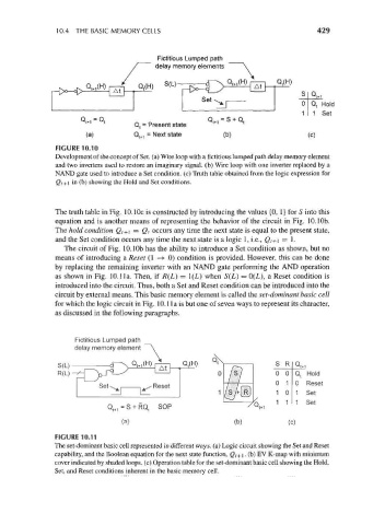
10.4 THE BASIC MEMORY CELLS                                          429


                                             Fictitious Lumped path
                                            delay memory elements


                                                                                     Q t Hold
                                                                                   . 1 Set
                         Q t+1 = Q,                       CL, = S + Q.
                          1 1                               1
                               '       Q, = Present state  *       '
                          (a)         Q t+1 = Next state      (b)                   (c)
                  FIGURE 10.10
                  Development of the concept of Set. (a) Wire loop with a fictitious lumped path delay memory element
                  and two inverters used to restore an imaginary signal, (b) Wire loop with one inverter replaced by a
                  NAND gate used to introduce a Set condition, (c) Truth table obtained from the logic expression for
                  Qt+i in (b) showing the Hold and Set conditions.


                  The truth table in Fig. lO.lOc is constructed by introducing the values {0, 1} for S into this
                  equation and is another means of representing the behavior of the circuit in Fig. 10.1Gb.
                  The hold condition Q t+\ = Qt occurs any time the next state is equal to the present state,
                  and the Set condition occurs any time the next state is a logic 1, i.e., Q t+\ = 1.
                    The circuit of Fig. lO.lOb has the ability to introduce a Set condition as shown, but no
                  means of introducing a Reset (1 -» 0) condition is provided. However, this can be done
                  by replacing the remaining inverter with an NAND gate performing the AND operation
                  as shown in Fig. 10.1 la. Then, if R(L) = 1(L) when S(L) = 0(L), a Reset condition is
                  introduced into the circuit. Thus, both a Set and Reset condition can be introduced into the
                  circuit by external means. This basic memory element is called the set-dominant basic cell
                  for which the logic circuit in Fig. 10.1 la is but one of seven ways to represent its character,
                  as discussed in the following paragraphs.


                        Fictitious Lumped path
                        delay memory element
                                                    Q t(H)   <>—^—i         s R
                                                                            0 0 Q t Hold
                                                                            0 1 0 Reset
                                                                            1 0 1 Set
                                                                            1 1 1 Set
                                Q t+1 = S + RQ t SOP
                                    (a)                          (b)           (c)
                  FIGURE 10.11
                  The set-dominant basic cell represented in different ways, (a) Logic circuit showing the Set and Reset
                  capability, and the Boolean equation for the next state function, Q t+i- (b) EV K-map with minimum
                  cover indicated by shaded loops, (c) Operation table for the set-dominant basic cell showing the Hold,
                  Set, and Reset conditions inherent in the basic memory cell.