
Page 464 - Engineering Digital Design
P. 464
434 CHAPTER 10 / INTRODUCTION TO SYNCHRONOUS STATE MACHINE DESIGN
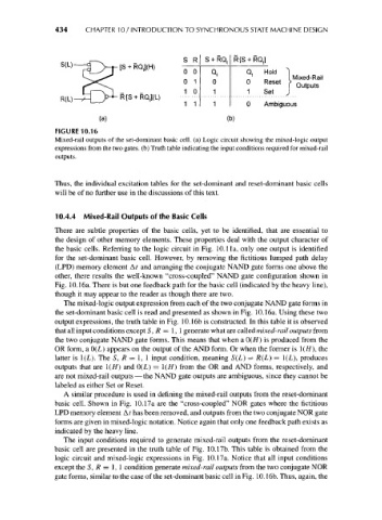
S R S + RQ, R-[S + RQ,]
[S + RQJ(H)
0 0 Q, Q. Hold
0 1 0 0 Reset I Mixed-Rail
I Outputs
1 0 1 1 Set J
R-[S + RQ t](L)
1 1 1 0 Ambiguous
(a) (b)
FIGURE 10.16
Mixed-rail outputs of the set-dominant basic cell, (a) Logic circuit showing the mixed-logic output
expressions from the two gates, (b) Truth table indicating the input conditions required for mixed-rail
outputs.
Thus, the individual excitation tables for the set-dominant and reset-dominant basic cells
will be of no further use in the discussions of this text.
10.4.4 Mixed-Rail Outputs of the Basic Cells
There are subtle properties of the basic cells, yet to be identified, that are essential to
the design of other memory elements. These properties deal with the output character of
the basic cells. Referring to the logic circuit in Fig. 10.1 la, only one output is identified
for the set-dominant basic cell. However, by removing the fictitious lumped path delay
(LPD) memory element At and arranging the conjugate NAND gate forms one above the
other, there results the well-known "cross-coupled" NAND gate configuration shown in
Fig. 10.16a. There is but one feedback path for the basic cell (indicated by the heavy line),
though it may appear to the reader as though there are two.
The mixed-logic output expression from each of the two conjugate NAND gate forms in
the set-dominant basic cell is read and presented as shown in Fig. 10.16a. Using these two
output expressions, the truth table in Fig. 10.16b is constructed. In this table it is observed
that all input conditions except S, R = 1,1 generate what are called mixed-rail outputs from
the two conjugate NAND gate forms. This means that when a 0(//) is produced from the
OR form, a 0(L) appears on the output of the AND form. Or when the former is !(//), the
latter is 1(L). The S, R = 1, I input condition, meaning S(L) = R(L) = l(L), produces
outputs that are l(H) and 0(L) = l(H) from the OR and AND forms, respectively, and
are not mixed-rail outputs — the NAND gate outputs are ambiguous, since they cannot be
labeled as either Set or Reset.
A similar procedure is used in defining the mixed-rail outputs from the reset-dominant
basic cell. Shown in Fig. 10.17a are the "cross-coupled" NOR gates where the fictitious
LPD memory element A/ has been removed, and outputs from the two conjugate NOR gate
forms are given in mixed-logic notation. Notice again that only one feedback path exists as
indicated by the heavy line.
The input conditions required to generate mixed-rail outputs from the reset-dominant
basic cell are presented in the truth table of Fig. 10.17b. This table is obtained from the
logic circuit and mixed-logic expressions in Fig. 10.17a. Notice that all input conditions
except the S, R = 1, 1 condition generate mixed-rail outputs from the two conjugate NOR
gate forms, similar to the case of the set-dominant basic cell in Fig. 10.16b. Thus, again, the