
Page 465 - Engineering Digital Design
P. 465
10.4 THE BASIC MEMORY CELLS 435
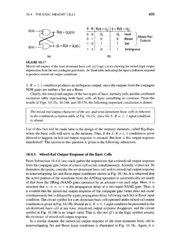
S R R(S + Q t) S + R(S + Q t)
0 0 Q Q Hold 1
* * I Mixed-Rail
0 1 0 0 Reset
f Outputs
1 0 1 1 Set J
S( H)
1 1 0 1 Ambiguous
(a) (b)
FIGURE 10.17
Mixed-rail outputs of the reset-dominant basic cell, (a) Logic circuit showing the mixed-logic output
expressions from the two confugate gate forms, (b) Truth table indicating the input conditions required
to produce mixed-rail output conditions.
S, R = 1, 1 condition produces an ambiguous output, since the outputs from the conjugate
NOR gates are neither a Set nor a Reset.
Clearly, the mixed-rail outputs of the two types of basic memory cells and the combined
excitation table representing both basic cells all have something in common. From the
results of Figs. 10.15c, 10.16b, and 10.17b, the following important conclusion is drawn:
The mixed-rail output character of the set- and reset-dominant basic cells is inherent
in the combined excitation table of Fig. 10.15c, since the S, R = 1, 1 input condition
is absent.
Use of this fact will be made later in the design of the memory elements, called flip-flops,
where the basic cells will serve as the memory. Thus, if the 5, R = 1, 1 condition is never
allowed to happen, mixed-rail output response is ensured. But how is this output response
manifested? The answer to this question is given in the following subsection.
10.4.5 Mixed-Rail Output Response of the Basic Cells
From Subsection 10.4.4, one could gather the impression that a mixed-rail output response
from the conjugate gate forms of a basic cell occurs simultaneously. Actually, it does not. To
dramatize this point, consider the set-dominant basic cell and its mixed-rail output response
to nonoverlapping Set and Reset input conditions shown in Fig. 10.18a. It is observed that
the active portion of the waveform from the ANDing operation is symmetrically set inside
of that from the ORing (NAND gate) operation by an amount i on each edge. Here, it is
assumed that T\ = 12 = T is the propagation delay of a two-input NAND gate. Thus, it
is evident that the mixed-rail output response of the conjugate gate forms does not occur
simultaneously but is delayed by a gate propagation delay following each Set or Reset input
condition. The circuit symbol for a set-dominant basic cell operated under mixed-rail output
conditions is given in Fig. 10.18b. Should an S, R = 1, 1 input condition be presented to the
set-dominant basic cell at any time, mixed-rail output response disappears, and the circuit
symbol in Fig. 10.18b is no longer valid. That is, the two <2's in the logic symbol assume
the existence of mixed-rail output response.
In a similar manner, the mixed-rail output response of the reset-dominant basic cell to
nonoverlapping Set and Reset input conditions is illustrated in Fig. 10.18c. Again, it is