
Page 461 - Engineering Digital Design
P. 461
10.4 THE BASIC MEMORY CELLS 431
holds as it must. But all branching conditions are easily deduced from an inspection of the
operation table. For example, the Set condition is the Boolean sum SR + SR = S, or the
Set Hold condition is the sum SR±SR + SR = S + R, which is simply the complement
of the Reset branching condition SR = S + R in agreement with the sum rule.
From the state diagram of Fig. 10.12a another important table is derived, called the
excitation table, and is presented in Fig. 10.12b. Notice that a don't care 0 is placed in
either the S or R column of the excitation table for the basic cell to indicate an unspecified
input branching condition. For example, the Set branching condition S requires that a 1 be
placed in the S column while a 0 is placed in the R column, indicating that R is not specified
in the branching condition for Set. Similarly, for the Set Hold branching path 1 -» 1, the
branching condition S + R requires a 1 and 0 to be placed in the S and R columns for the S
portion of the branching condition, and that a 0 and 0 to be placed in the S and R columns
for the R portion, respectively. Thus, the excitation table specifies the input logic values for
each of the four corresponding state variable changes in the state diagram as indicated.
As a seventh and final means of representing the behavior of the set-dominant basic cell,
a timing diagram can be constructed directly from the operation table in Fig. 10.1 Ic. This
timing diagram is given in Fig. 10.12c, where the operating conditions Set, Set Hold, Reset,
and Reset Hold are all represented—at this point no account is taken of the path delay
through the gates. Notice that the set-dominant character is exhibited by the S, R = 1,0
and S, R = 1, 1 input conditions in both the operation table and timing diagram.
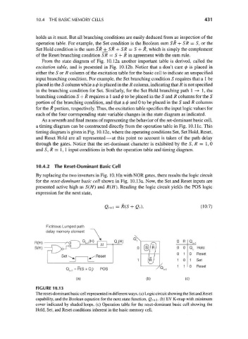
10.4.2 The Reset-Dominant Basic Cell
By replacing the two inverters in Fig. lO.lOa with NOR gates, there results the logic circuit
for the reset-dominant basic cell shown in Fig. 10.13a. Now, the Set and Reset inputs are
presented active high as S(H) and R(H). Reading the logic circuit yields the POS logic
expression for the next state,
= R(S + Gr), (10.7)
Fictitious Lumped path
delay memory element
Q,(H) w '\ S R Q t+i
0 0 Q, Hold
0 1 0 Reset
1 0 1 Set
1 1 0 Reset
Q t+1 = R(S + Q t) POS
(a) (b) (c)
FIGURE 10.13
The reset-dominant basic cell represented in different ways, (a) Logic circuit showing the Set and Reset
capability, and the Boolean equation for the next state function, Q t+\. (b) EV K-map with minimum
cover indicated by shaded loops, (c) Operation table for the reset-dominant basic cell showing the
Hold, Set, and Reset conditions inherent in the basic memory cell.