
Page 469 - Engineering Digital Design
P. 469
10.5 INTRODUCTION TO FLIP-FLOPS 439
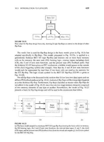
FIGURE 10.21
Flow chart for flip-flop design hierarchy, showing D type flip-flops as central to the design of other
flip-flops.
The model that is used for flip-flop design is the basic model given in Fig. 10.3c but
adapted specifically to flip-flops. This model, presented in Fig. 10.22a, is applied to a
generalized, fictitious RET XY type flip-flop and features one or more basic memory
cells as the memory, the next state (NS) forming logic, external inputs including clock
(CK), the S and R next state functions, and the present state (PS) feedback paths. Had
the fictitious XY-FF been given an FET mechanism, a bubble would appear on the outside
of the clock triggering symbol (the triangle). Note that the S and R next state functions
would each be represented by dual lines if two basic cells are used as the memory for
the XY flip-flop. The logic circuit symbol for the RET XY flip-flop (XY-FF) is given in
Fig. 10.22b.
Not all flip-flops to be discussed in the sections that follow have two data inputs and not
all have PS feedback paths as in Fig. 10.22. And not all flip-flops will be rising edge triggered
as in this fictitious flip-flop. Furthermore, flip-flops classified as master-slave flip-flops do
not adhere to the model of Fig. 10.22, since they are two-stage memory elements composed
of two memory elements of one type or another. Nevertheless, the model of Fig. 10.22
presents a basis for flip-flop design and will be used in the discussions that follow.
(a) (b)
FIGURE 10.22
(a) The basic model adapted to a fictitious RET XY type flip-flop showing the basic cell(s) as memory,
the NS forming logic, the S and R next state fucntions, the external data inputs X and Y, the clock
(CK) input, and the present state (PS) feedback lines from the mixed-rail outputs Q. (b) Circuit symbol
for the RET XY flip-flop.