
Page 474 - Engineering Digital Design
P. 474
444 CHAPTER 10 / INTRODUCTION TO SYNCHRONOUS STATE MACHINE DESIGN
D+CK
lfCK = 0, Q follows D.
.-. Transparent
NS Logic Memory
/-
D(H) , „-« N . Q(H) j
D+CK
(a) (b) (c)
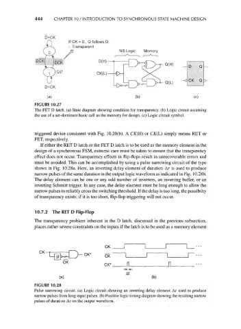
FIGURE 10.27
The FET D latch, (a) State diagram showing condition for transparency, (b) Logic circuit assuming
the use of a set-dominant basic cell as the memory for design, (c) Logic circuit symbol.
triggered device consistent with Fig. 10.20(b). A CK(H) or CK(L) simply means RET or
FET, respectively.
If either the RET D latch or the FET D latch is to be used as the memory element in the
design of a synchronous FSM, extreme care must be taken to ensure that the transparency
effect does not occur. Transparency effects in flip-flops result in unrecoverable errors and
must be avoided. This can be accomplished by using a pulse narrowing circuit of the type
shown in Fig. 10.28a. Here, an inverting delay element of duration A? is used to produce
narrow pulses of the same duration in the output logic waveform as indicated in Fig. 10.28b.
The delay element can be one or any odd number of inverters, an inverting buffer, or an
inverting Schmitt trigger. In any case, the delay element must be long enough to allow the
narrow pulses to reliably cross the switching threshold. If the delay is too long, the possibilty
of transparency exists; if it is too short, flip-flop triggering will not occur.
10.7.2 The RET D Flip-Flop
The transparency problem inherent in the D latch, discussed in the previous subsection,
places rather severe constraints on the inputs if the latch is to be used as a memory element
At
(a) (b)
FIGURE 10.28
Pulse narrowing circuit, (a) Logic circuit showing an inverting delay element Ar used to produce
narrow pulses from long input pulses, (b) Positive logic timing diagram showing the resulting narrow
pulses of duration At on the output waveform.