
Page 479 - Engineering Digital Design
P. 479
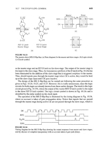
10.7 THE D FLIP-FLOPS: GENERAL                                       449


                                                                 Master        Slave
                       D+CK             -„.-.-          D(H)
                                                                D    Q  -^-   D   Q -Q(H)
                                                         CK     CK   Q ,   fCK    Q  D-Q(L)


                                                                         (b)


                      D + CK
                    RET D Latch      FET D Latch
                    Master Stage     Slave Stage

                                (a)                                      (c)
                  FIGURE 10.33
                  The master-slave (MS) D flip-flop, (a) State diagram for the master and slave stages, (b) Logic circuit,
                  (c) Circuit symbol.


                  as the master stage and an FET D latch as the slave stage. The output of the master stage is
                  the input to the slave stage. Thus, the transparency problem of the D latch in Fig. 10.24a has
                  been eliminated by the addition of the slave stage that is triggered antiphase to the master.
                  Thus, should signals pass through the master stage when CK is active, they would be held
                  up at the slave stage input until CK goes inactive.
                    The design of the MS D flip-flop can be carried out following the same procedure as
                  given in Figs. 10.24, 10.25, and 10.27. However, this is really unnecessary, since the logic
                  circuits for both stages are already known from these earlier designs. The result is the logic
                  circuit given in Fig. 10.33b, where the output of the master RET D latch symbol is the input
                  to the slave FET D latch symbol. The logic circuit symbol is shown in Fig. 10.33c and is
                  identified by the pulse symbol on the clock input.
                    The operation of the MS D flip-flop is illustrated by the timing diagram in Fig. 10.34,
                  where no account is taken of gate propagation delay. Notice that signals that are passed
                  through the master stage during active CK are not passed through the slave stage, which is


                       CK

                       D(H)


                       Q(H)

                  FIGURE 10.34
                  Timing diagram for the MS D flip-flop showing the output response from master and slave stages,
                  and the absence of complete transparency with no account taken of gate path delays.