
Page 480 - Engineering Digital Design
P. 480
450 CHAPTER 10 / INTRODUCTION TO SYNCHRONOUS STATE MACHINE DESIGN
(a) (b)
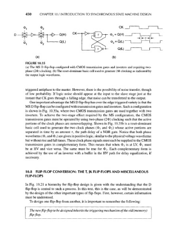
FIGURE 10.35
(a) The MS D flip-flop configured with CMOS transmission gates and inverters and requiring two-
phase (2<t>) clocking, (b) The reset-dominant basic cell used to generate 2<I> clocking as indicated by
the output logic waveforms.
triggered antiphase to the master. However, there is the possibility of noise transfer, though
of low probability. If logic noise should appear at the input to the slave stage just at the
instant that CK goes through a falling edge, that noise can be transferred to the output.
One important advantage the MS D flip-flop has over the edge triggered variety is that the
MS D flip-flop can be configured with transmission gates and inverters. Such a configuration
is shown in Fig. 10.35a, where two CMOS transmission gates are used together with two
inverters. To achieve the two-stage effect required by the MS configuration, the CMOS
transmission gates must be operated by using two-phase (24>) clocking such that the active
portions of the clock phases are nonoverlapping. Shown in Fig. 10.35b is a reset-dominant
basic cell used to generate the two clock phases (<&\ and $2) whose active portions are
separated in time by an amount r, the path delay of a NOR gate. Notice that both phase
waveforms (4> i and 4> 2) are given in positive logic, similar to the physical voltage waveforms
but without rise and fall times. These clock phase signals must each be supplied to the CMOS
transmission gates in complementary form. This means that when 4>i is at LV, <I>i must
be at HV and vice versa. The same must be true for 4> 2- Each complementary form is
achieved by the use of an inverter with a buffer in the HV path for delay equalization, if
necessary.
10.8 FLIP-FLOP CONVERSION: THE T, JK FLIP-FLOPS AND MISCELLANEOUS
FLIP-FLOPS
In Fig. 10.21 a hierarchy for flip-flop design is given with the understanding that the D
flip-flop is central to such a process. In this text, this is the case, as will be demonstrated
by the design of the other important types of flip-flops. First, however, certain information
must be understood.
To design one flip-flop from another, it is important to remember the following:
The new flip-flop to be designed inherits the triggering mechanism of the old (memory)
flip-flop.