
Page 485 - Engineering Digital Design
P. 485
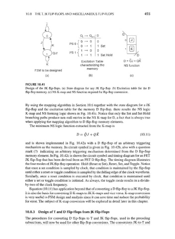
10.8 THE T,JK FLIP-FLOPS AND MISCELLANEOUS FLIP-FLOPS                455


                                                  Q t -» <Vi  D
                                                  o -> o   0
                                            PSO
                                                  0 -» 1    1 Set
                                                  1 -»• 0  0
                                  CUT       PS 1
                                                  1 -+ 1   1 Set Hold           / D
                                                  Excitation Table        D = QJ + QK
                              K
                                                  characterizing the       NS function
                        FSM to be designed                 ^
                              (a)                      (b)                    (c)
                  FIGURE 10.41
                  Design of the JK flip-flops, (a) State diagram for any JK flip-flop, (b) Excitation table for the D
                  flip-flop memory, (c) NS K-map and NS function required for flip-flop conversion.


                  By using the mapping algorithm in Section 10.6 together with the state diagram for a JK
                  flip-flop and the excitation table for the memory D flip-flop, there results the NS logic
                  K-map and NS forming logic shown in Fig. 10.41c. Notice that only the Set and Set Hold
                  branching paths produce non-null entries in the NS K-map for D, a fact that is always true
                  when applying the mapping algorithm to D flip-flop memory elements.
                    The minimum NS logic function extracted from the K-map is

                                               D=QJ + QK                            (10.11)

                  and is shown implemented in Fig. 10.42a with a D flip-flop of an arbitrary triggering
                  mechanism as the memory. Its circuit symbol is given in Fig. 10.42b, also with a question
                  mark (?) indicating an arbitrary triggering mechanism determined from the D flip-flop
                  memory element. In Fig. 10.42c is shown the circuit symbol and timing diagram for an FET
                  JK flip-flop that has been derived from an FET D flip-flop. The timing diagram illustrates
                  the four modes of JK flip-flop operation: Hold (Reset or Set), Reset, Set, and Toggle. Notice
                  that once a set condition is sampled by clock, that condition is maintained by the flip-flop
                  until either a reset or toggle condition is sampled by the falling edge of the clock waveform.
                  Similarly, once a reset condition is executed by clock, that condition is maintained until
                  either a set or toggle condition is initiated. As always, the toggle mode results in a divide-
                  by-two of the clock frequency.
                    Equation (10.11) has application beyond that of converting a D flip-flop to a JK flip-flop.
                  It is also the basis for converting D K-maps to JK K-maps and vice versa. K-map conversion
                  is very useful in FSM design and analysis since it can save time and reduce the probability
                  for error. The subject of K-map conversion will be explored in detail later in this chapter.


                  10.8.3 Design of T and D Flip-Flops from JK Flip-Flops
                  The procedures for converting D flip-flops to T and JK flip-flops, used in the preceding
                  subsections, will now be used for other flip-flop conversions. The conversions JK-to-T and