
Page 489 - Engineering Digital Design
P. 489
10.8 THE TJK FLIP-FLOPS AND MISCELLANEOUS FLIP-FLOPS 459
S T 0 -> 0 0
PS 0
w
0 0 0 Reset /~* \ Q -> 1 1 Set
T
0 1 Q t Toggle ^ S + ( r 1 -, o 0
1 0 1 Set \ / \ 1 -. 1 1 Set Hold
1 1 1 Set
Excitation Table
Operation (J characterizing the
Table S memor V
a
c
( ) State Diagram ( )
(b)
D = S + QT
(d) (e)
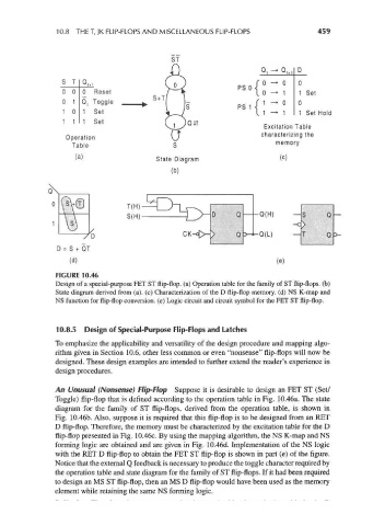
FIGURE 10.46
Design of a special-purpose FET ST flip-flop, (a) Operation table for the family of ST flip-flops, (b)
State diagram derived from (a), (c) Characterization of the D flip-flop memory, (d) NS K-map and
NS function for flip-flop conversion, (e) Logic circuit and circuit symbol for the FET ST flip-flop.
10.8.5 Design of Special-Purpose Flip-Flops and Latches
To emphasize the applicability and versatility of the design procedure and mapping algo-
rithm given in Section 10.6, other less common or even "nonsense" flip-flops will now be
designed. These design examples are intended to further extend the reader's experience in
design procedures.
An Unusual (Nonsense) Flip-Flop Suppose it is desirable to design an FET ST (Set/
Toggle) flip-flop that is defined according to the operation table in Fig. 10.46a. The state
diagram for the family of ST flip-flops, derived from the operation table, is shown in
Fig. 10.46b. Also, suppose it is required that this flip-flop is to be designed from an RET
D flip-flop. Therefore, the memory must be characterized by the excitation table for the D
flip-flop presented in Fig. 10.46c. By using the mapping algorithm, the NS K-map and NS
forming logic are obtained and are given in Fig. 10.46d. Implementation of the NS logic
with the RET D flip-flop to obtain the FET ST flip-flop is shown in part (e) of the figure.
Notice that the external Q feedback is necessary to produce the toggle character required by
the operation table and state diagram for the family of ST flip-flops. If it had been required
to design an MS ST flip-flop, then an MS D flip-flop would have been used as the memory
element while retaining the same NS forming logic.