
Page 487 - Engineering Digital Design
P. 487
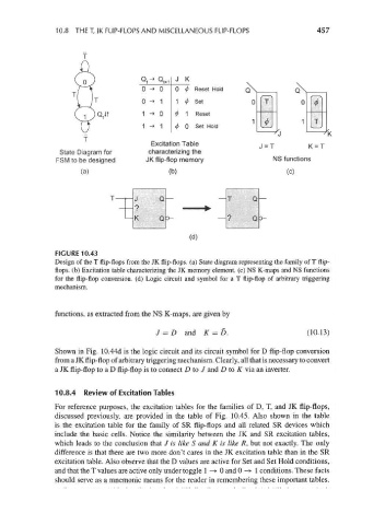
10.8 THE T, JK FLIP-FLOPS AND MISCELLANEOUS FLIP-FLOPS               457


                                                 J K
                                             0*1
                                        o -» o   0  <j> Reset Hold
                                        0 -» 1   1 ^ Set
                                        1 -» 0   ^ 1 Reset
                                        1 -» 1   ^ 0 Set Hold

                                           Excitation Table            J= T        K= T
                   State Diagram for      characterizing the
                  FSM to be designed     JK flip-flop memory              NS functions
                        (a)                    (b)                            (c)


                                                     (d)
                  FIGURE 10.43
                  Design of the T flip-flops from the JK flip-flops, (a) State diagram representing the family of T flip-
                  flops, (b) Excitation table characterizing the JK memory element, (c) NS K-maps and NS functions
                  for the flip-flop conversion, (d) Logic circuit and symbol for a T flip-flop of arbitrary triggering
                  mechanism.


                  functions, as extracted from the NS K-maps, are given by

                                            J = D and K = D.                        (10.13)

                  Shown in Fig. 10.44d is the logic circuit and its circuit symbol for D flip-flop conversion
                  from a JK flip-flop of arbitrary triggering mechanism. Clearly, all that is necessary to convert
                  a JK flip-flop to a D flip-flop is to connect D to J and D to K via an inverter.


                  10.8.4 Review of Excitation Tables
                  For reference purposes, the excitation tables for the families of D, T, and JK flip-flops,
                  discussed previously, are provided in the table of Fig. 10.45. Also shown in the table
                  is the excitation table for the family of SR flip-flops and all related SR devices which
                  include the basic cells. Notice the similarity between the JK and SR excitation tables,
                  which leads to the conclusion that J is like S and K is like R, but not exactly. The only
                  difference is that there are two more don't cares in the JK excitation table than in the SR
                  excitation table. Also observe that the D values are active for Set and Set Hold conditions,
                  and that the T values are active only under toggle 1 -> 0 and 0 -> 1 conditions. These facts
                  should serve as a mnemonic means for the reader in remembering these important tables.