
Page 483 - Engineering Digital Design
P. 483
10.8 THE TJK FLIP-FLOPS AND MISCELLANEOUS FLIP-FLOPS 453
Inherits triggering
of the D flip-flop
Indicates an arbitrary
a) triggering mechanism
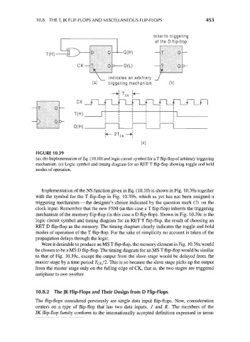
FIGURE 10.39
(a), (b) Implementation of Eq. (10.10) and logic circuit symbol for a T flip-flop of arbitrary triggering
mechanism, (c) Logic symbol and timing diagram for an RET T flip-flop showing toggle and hold
modes of operation.
Implementation of the NS function given in Eq. (10.10) is shown in Fig. 10.39a together
with the symbol for the T flip-flop in Fig. 10.39b, which as yet has not been assigned a
triggering mechanism — the designer's choice indicated by the question mark (?) on the
clock input. Remember that the new FSM (in this case a T flip-flop) inherits the triggering
mechanism of the memory flip-flop (in this case a D flip-flop). Shown in Fig. 10.39c is the
logic circuit symbol and timing diagram for an RET T flip-flop, the result of choosing an
RET D flip-flop as the memory. The timing diagram clearly indicates the toggle and hold
modes of operation of the T flip-flop. For the sake of simplicity no account is taken of the
propagation delays through the logic.
Were it desirable to produce an MS T flip-flop, the memory element in Fig. 10.39a would
be chosen to be a MS D flip-flop. The timing diagram for an MS T flip-flop would be similar
to that of Fig. 10.39c, except the output from the slave stage would be delayed from the
master stage by a time period TCK!^- This is so because the slave stage picks up the output
from the master stage only on the falling edge of CK, that is, the two stages are triggered
antiphase to one another.
10.8.2 The JK Flip-Flops and Their Design from D Flip-Flops
The flip-flops considered previously are single data input flip-flops. Now, consideration
centers on a type of flip-flop that has two data inputs, J and K. The members of the
JK flip-flop family conform to the internationally accepted definition expressed in terms