
Page 478 - Engineering Digital Design
P. 478
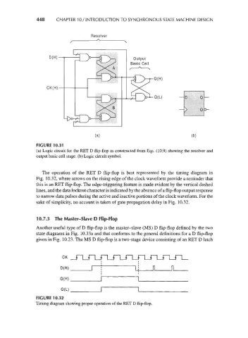
448     CHAPTER 10 / INTRODUCTION TO SYNCHRONOUS STATE MACHINE DESIGN


                                          Resolver


                         D(H)


                                                                   -Q(H)
                                              ~~          k"-^
                        CK(H)-
                                              _           rv-^N
                                                                   •Q(L)


                                           (a)                                    (b)
                     FIGURE 10.31
                     (a) Logic circuit for the RET D flip-flop as constructed from Eqs. (10.9) showing the resolver and
                     output basic cell stage, (b) Logic circuit symbol.


                       The operation of the RET D flip-flop is best represented by the timing diagram in
                     Fig. 10.32, where arrows on the rising edge of the clock waveform provide a reminder that
                     this is an RET flip-flop. The edge-triggering feature is made evident by the vertical dashed
                     lines, and the data lockout character is indicated by the absence of a flip-flop output response
                     to narrow data pulses during the active and inactive portions of the clock waveform. For the
                     sake of simplicity, no account is taken of gate propagation delay in Fig. 10.32.


                     10.7.3 The Master-Slave D Flip-Flop
                     Another useful type of D flip-flop is the master-slave (MS) D flip-flop defined by the two
                     state diagrams in Fig. 10.33a and that conforms to the general definitions for a D flip-flop
                     given in Fig. 10.23. The MS D flip-flop is a two-stage device consisting of an RET D latch


                               CK

                               D(H)

                              Q(H)
                               Q(L)
                     FIGURE 10.32
                    Timing diagram showing proper operation of the RET D flip-flop.