
Page 475 - Engineering Digital Design
P. 475
10.7 THE D FLIP-FLOPS: GENERAL 445
S+R
(b) Basic Cell
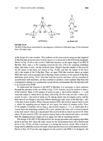
FIGURE 10.29
The RET D flip-flop as represented by state diagrams, (a) Resolver FSM input stage, (b) Set-dominant
basic cell output stage.
in the design of a state machine. This problem can be overcome by using an edge triggered
D flip-flop that possesses data lockout character as discussed in the following paragraph.
Shown in Fig. 10.29a is the resolver FSM that functions as the input stage of an RET D
flip-flop. Here, state a is the sampling (unresolved) state, CK is the sampling (enabling)
input, and states b and c are the resolved states. Observe that the outputs of the resolver
are the inputs to the basic cell shown in Fig. 10.29b, and that the output of the basic
cell is the output of the D flip-flop. Thus, an input FSM (the resolver) drives an output
FSM (the basic cell) to produce the D flip-flop which conforms to the general D flip-flop
definitions given in Fig. 10.23. Note that both the resolver and basic cell are classified as
asynchronous state machines, yet they combine to produce a state machine (flip-flop) that
is designed to operate in a synchronous (clock-driven) environment. But the flip-flop itself
is an asynchronous FSM!
To understand the function of the RET D flip-flop, it is necessary to move stepwise
through the operation of the two FSMs in Fig. 10.29: Initially, let Q be inactive in state a
of the resolver. Then, if CK samples D active in state a, the resolver transits a —>• c and
issues the output S, which drives the basic cell in Fig. 10.29b to the set state 1 where Q is
issued. In state c, the resolver holds on CK, during which time Q remains active; and the
data input D can change at any time without altering the logic status of the flip-flop — this
is the data lockout feature. When CK goes inactive (CK), the resolver transits back to state
a, where the sampling process begins all over again, but where Q remains active. Now,
if CK samples D inactive (D) in state a, the resolver transits a ->• b, at which time R is
issued. Since the branching condition SR is now satisfied, the basic cell is forced to transit
to the reset state 0, where Q is deactivated. The resolver holds in state b on active CK. Then
when CK goes inactive (CK), the resolver transits back to the unresolved state a, at which
time the sampling process begins all over again, but with Q remaining inactive.
The design of the RET D flip-flop follows the design procedure and mapping algorithm
given in Section 10.6. Since the logic circuit for the set-dominant basic cell is known and
given in Fig. 10.18a, all that is necessary is to design the resolver circuit. This is done by
using what is called the nested cell model, which uses the basic cells as the memory elements.
Shown in Fig. 10.30 are the state diagram for the resolver (the FSM to be designed), the