
Page 477 - Engineering Digital Design
P. 477
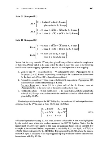
10.7 THE D FLIP-FLOPS: GENERAL                                       447


                  Stated (K-mapcelM)

                                    1 0 -» 0, place 0 in the S A K-map, I }
                                            place 0 in the RA K-map I

                                      1 -> 0, place 1 • (CK) = CKin the R B K-map )
                                                                            >
                                      1 -» 1, place 0 • (CK) = (f>CK in the S B K-map]
                                    !

                  State 10 (K-map cell 2)
                                    (  1 ->• 0, place 1 • (CK) = CK in the R A K-map 1

                                      1 -> 1, place 0 • (CK) = 0C£ in the 5 A K-map j
                                    (  0 -» 0, place 0 in the S B K-map, 1
                                                              F> i
                                           . F
                                                        «
                                            place 0 in the /? s K-map I
                  Notice that for every essential EV entry in a given K-map cell there exists the complement
                  of that entry ANDed with 0 in the same cell of the other K-map. This leads to the following
                  modification of the mapping algorithm in Section 10.6 as it pertains to S/R mapping:

                    1. Look for Sets (0 -> 1) and Resets (1 -» 0) and make the entry 1-(Appropriate BC) in
                       the proper Sj or /?,- K-map, respectively, according to the combined excitation table
                       for the basic cell. (Note: BC = branching condition.)
                    2. For each Set entry (from [ 1 ]) in a given cell of the 5, K-map, enter 0 • (Appropriate BC)
                       in the same cell of the corresponding /?, K-map.
                       For each Reset entry (from [1]) in a given cell of the /?, K-map, enter 0-
                       (Appropriate BC) in the same cell of the corresponding 5,- K-map.
                    3. For Hold Resets (0 -> 0) and Hold Sets (1 -> 1), enter (0,0) and (0,0), respectively,
                       in the (S,,/?,) K-maps in accordance with the combined excitation table for basic cell
                       given in Fig. 10.15c.

                    Continuing with the design of the RET D flip-flop, the minimum NS and output functions
                  extracted from the EV K-maps in Figs. 10.30c and 10.30d are

                                          S  = BDCK      R A
                                           A
                                          S  = ADCK      R B                         (10.9)
                                           B
                                               S = A R = B

                  which are implemented in Fig. 10.31a. Here, the basic cells for bits A and B are highlighted
                  by the shaded areas within the resolver section of the RET D flip-flop. Notice that the
                  requirement of active low inputs to the three set-dominant basic cells is satisfied. For
                  example, in the resolver FSM this requirement is satisfied by R A(L) = Rs(L) = CK(L) =
                  CK(H). The circuit symbol for the RET D flip-flop is given in Fig. 10.3 Ib, where the triangle
                  on the CK input is indicative of an edge triggered flip-flop with data-lockout character and
                  is consistent with Fig. 10.20a.