Page 476 - Engineering Digital Design
P. 476

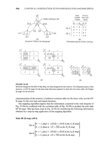
446     CHAPTER 10/INTRODUCTION TO SYNCHRONOUS STATE MACHINE DESIGN


                                                                           State  Memory
                                                                          variable input logic
                                             State varibales AB           change  values

                                                                        Q t -> Q t+1 S R
                                                                         0^ 0     0  (f>
                                                                         0 -> 1   1 0
                                                                         1 -> 0   0 1

                             PIT
                                       (a)                                    (b)
                             Resolver FSM to be designed           Characterization of the memory


                            DCK

                                                  CK
                                                               /
                                                             7R,
                                        /S A
                                                  u
                                                                         0  1      0   1
                            DCK                 ^(D+CKL   CK          A^ 0  0  0  ^
                                                                                 0 0
                                                   </>         /       1 (T~ Tl  /  1 n  w
                                        TS                                   X S
                                         &
                                         B                    /R 0
                                           (c)                                (d)
                     FIGURE 10.30
                     Resolver design for the RET D flip-flop, (a) State diagram for the resolver. (b) Characterization of the
                     memory, (c) EV K-maps for the next state functions required to drive the two basic cells, (d) Output
                     K-maps for the resolver.


                     characterization of the memory (combined excitation table for the basic cell), and the EV
                     K-maps for the next state and output functions.
                       The mapping algorithm requires that the information contained in the state diagram of
                    Fig. 10.30a be combined with the excitation table of Fig. 10.30b to produce the next state
                    EV K-maps. This has been done in Fig. 10.30c by introducing the following information
                    obtained by a step-by-step application of the mapping algorithm:


                     State 00 (K-map cell 0)

                                       [
                                       0 -> 1, place 1 • (DCK) = DCK in the 5 A K-map 1
                                 Bit A {              -                        }
                                      '0^0, place 0 • (D + CK) in the R A K-map  ]
                                          > 1, place 1 • (DCK) = DCK in the S B K-map 1
                                          > 0, place 0 • (D + CK) in the R B K-map  I
   471   472   473   474   475   476   477   478   479   480   481