
Page 481 - Engineering Digital Design
P. 481
10.8 THE TJK FLIP-FLOPS AND MISCELLANEOUS FLIP-FLOPS 451
Fictitious
1 XY-FF
1 . x
NS »• D Q L-Q(H) _ V Q
Forming Memory
Logic
-* ? Q D— - Q(L) -^? Q
V /
\ He
CK \— triggering mechanism —'
of XY flip-flop
(a) (b)
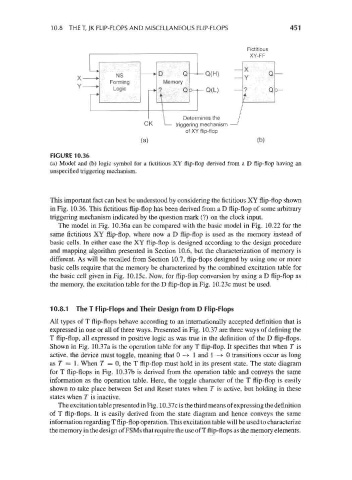
FIGURE 10.36
(a) Model and (b) logic symbol for a fictitious XY flip-flop derived from a D flip-flop having an
unspecified triggering mechanism.
This important fact can best be understood by considering the fictitious XY flip-flop shown
in Fig. 10.36. This fictitious flip-flop has been derived from a D flip-flop of some arbitrary
triggering mechanism indicated by the question mark (?) on the clock input.
The model in Fig. 10.36a can be compared with the basic model in Fig. 10.22 for the
same fictitious XY flip-flop, where now a D flip-flop is used as the memory instead of
basic cells. In either case the XY flip-flop is designed according to the design procedure
and mapping algorithm presented in Section 10.6, but the characterization of memory is
different. As will be recalled from Section 10.7, flip-flops designed by using one or more
basic cells require that the memory be characterized by the combined excitation table for
the basic cell given in Fig. 10.15c. Now, for flip-flop conversion by using a D flip-flop as
the memory, the excitation table for the D flip-flop in Fig. 10.23c must be used.
10.8.1 The T Flip-Flops and Their Design from D Flip-Flops
All types of T flip-flops behave according to an internationally accepted definition that is
expressed in one or all of three ways. Presented in Fig. 10.37 are three ways of defining the
T flip-flop, all expressed in positive logic as was true in the definition of the D flip-flops.
Shown in Fig. 10.37a is the operation table for any T flip-flop. It specifies that when T is
active, the device must toggle, meaning that 0 -> 1 and 1 -> 0 transitions occur as long
as T = 1. When T = 0, the T flip-flop must hold in its present state. The state diagram
for T flip-flops in Fig. 10.37b is derived from the operation table and conveys the same
information as the operation table. Here, the toggle character of the T flip-flop is easily
shown to take place between Set and Reset states when T is active, but holding in these
states when T is inactive.
The excitation table presented in Fig. 10.37c is the third means of expressing the definition
of T flip-flops. It is easily derived from the state diagram and hence conveys the same
information regarding T flip-flop operation. This excitation table will be used to characterize
the memory in the design of FSMs that require the use of T flip-flops as the memory elements.