
Page 473 - Engineering Digital Design
P. 473
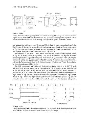
10.7 THE D FLIP-FLOPS: GENERAL                                       443


                                                       NS Logic  Memory
                                                                       \
                                                                          Q(H)    I


                                                                          Q(L)
                                           -
                                        ' •          *—\^>o-^—\ j~ '  i '
                                  R = DCK
                             (a)                               (b)                  (c)
                  FIGURE 10.25
                  Design of the RET D latch by using a basic cell as the memory, (a) EV K-maps and minimum Boolean
                  expressions for the S and ^? next-state functions, (b) Logic circuit showing the NS logic from part (a)
                  and the set-dominant basic cell as the memory, (c) Logic circuit symbol for the RET D latch.


                  use in extracting minimum cover. Note that DCK (in the S K-map) is contained in 0D, that
                  DCK (in the R K-map) is contained in 0D, and that the logic circuit conforms to the model
                  in Fig. 10.22 exclusive of PS feedback. The CK input to the circuit symbol in Fig. 10.25c
                  is consistent with that for a latch as indicated in Fig. 10.20a.
                    The behavior of the RET D latch is best demonstrated by the timing diagram shown
                  in Fig. 10.26. Here, normal D flip-flop (D-FF) action is indicated for D pulse durations
                  much longer than a CK period. For normal D-FF behavior, Q goes active when CK samples
                  (senses) D active, and Q goes inactive when CK samples D inactive. However, when CK is
                  active and D changes activation level, the transparency effect occurs. This is demonstrated
                  in the timing diagram of Fig. 10.26.
                    The FET (transparent low) D latch is designed in a similar manner to the RET D latch
                  just described. All that is required is to complement CK throughout in the state diagram
                  of Fig. 10.24a, as shown in Fig. 10.27a. Now, the transparency effect occurs when CK is
                  inactive (CK = 0). If a set-dominant basic cell is again used as the memory, there results the
                  logic circuit of Fig. 10.27b, where an inverter is the only added feature to the logic circuit
                  shown in Fig. 10.25b. The logic circuit symbol for the FET D latch is given in Fig. 10.27c.
                  Here, the active low indicator bubble on the clock input identifies this as a falling edge


                                                                 X
                             Normal D-FF action                    \_ '
                                                                    Transparency
                  FIGURE 10.26
                  Timing diagram for an RET D latch showing normal D-FF action and the transparency effect that can
                  occur when CK is active, where no account is taken of gate path delays.