
Page 490 - Engineering Digital Design
P. 490
460 CHAPTER 10/INTRODUCTION TO SYNCHRONOUS STATE MACHINE DESIGN
The external hardware requirememts in the design of the FET ST flip-flop can be min-
imized by using an RET JK flip-flop as the memory in place of a D flip-flop. If the D
excitation table in Fig. 10.46c is replaced by that for the JK flip-flops in Fig. 10.40c, the NS
functions become J = S + T and K = S, a reduction of one gate. It is left to the reader to
show the mapping details.
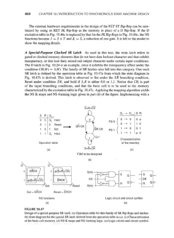
A Special-Purpose Clocked SR Latch As used in this text, the term latch refers to
gated or clocked memory elements that do not have data lockout character and that exhibit
transparency, or that lose their mixed-rail output character under certain input conditions.
The D latch in Fig. 10.24 is an example, since it exhibits the transparency effect under the
condition CK(H) = !(//). The family of SR latches also fall into this category. One such
SR latch is defined by the operation table in Fig. 10.47a from which the state diagram in
Fig. 10.47b is derived. This latch is observed to Set under the SR branching condition,
Reset under condition SR, and hold if S,R is either 0,0 or 1,1. Notice that CK is part
of the input branching conditions, and that the basic cell is to be used as the memory
characterized by the excitation table in Fig. 10.47c. Applying the mapping algorithm yields
the NS K-maps and NS-forming logic given in part (d) of the figure. Implementing with a
S+R+CK
Q. -> Q. +i S R
S R
Q w
0 0 Q, Hold v~ / p so 0 0
0 1 0 Reset „= ~, \ \ ^ ° 1 0
1 0 1 Set I ISR-CK PS1 J 1 -> 0 0 1
1 1 Q. Hold \—< X 1 -> 1 (p 0
Characterization
Operation table I^J of the memory
(a) S+R+CK (c)
FSM to be designed
(b)
NS functions Logic circuit and circuit symbol
(d) (e)
FIGURE 10.47
Design of a special-purpose SR latch, (a) Operation table for this family of SR flip-flops and latches,
(b) State diagram for the special SR latch derived from the operation table in (a), (c) Characterization
of the basic cell memory, (d) NS K-maps and NS-forming logic, (e) Logic circuit and circuit symbol.