
Page 495 - Engineering Digital Design
P. 495
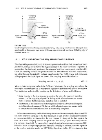
10.11  SETUP AND HOLD-TIME REQUIREMENTS OF FLIP-FLOPS               465


                         V      Sampling                      y     Sampling
                                 Interval                     A      Interval


                                            Active
                                         transition point
                                                                                Inactive
                                                                             transition point
                                             Mime                                -Mime
                   Inputs can —>-^  J^ ^—>• Inputs can  Inputs can —>•   •  —>• Inputs can
                    change     *~| **{*      change     change     "*~^—Mr*      change

                                  (a)                                  (b)
                  FIGURE 10.53
                  Clock voltage waveforms showing sampling interval (r su + ?h) during which time the data inputs must
                 remain stable at their proper logic levels, (a) Rising edge of the clock waveform, (b) Falling edge of
                 the clock waveform.


                  10.11  SETUP AND HOLD-TIME REQUIREMENTS OF FLIP-FLOPS

                 Flip-flops will operate reliably only if the data inputs remain stable at their proper logic levels
                 just before, during, and just after the triggering edge of the clock waveform. To put this in
                 perspective, the data inputs must meet the setup and hold-time requirements established by
                 clock, the sampling variable for synchronous FSMs. The setup and hold-time requirements
                 for a flip-flop are illustrated by voltage waveforms in Fig. 10.53, where both rising and
                 falling edges of the clock signal are shown. The sampling interval is defined as

                                         Sampling interval = (t su + ?/,),          (10.15)

                 where t su is the setup time and th is the hold time. It is during the sampling interval that the
                 data inputs must remain fixed at their proper logic level if the outcome is to be predictable.
                 This fact is best understood by considering the definitions of setup and hold times:

                    • Setup time t su is the time interval preceding the active (or inactive) transition
                      point (t tr) of the triggering edge of CK during which all data inputs must remain
                      stable to ensure that the intended transition will be initiated.
                    • Hold time f/, is the time interval following the active (or inactive) transition point
                      (t tr) of the triggering edge of CK during which all data inputs must remain stable
                      to ensure that the intended transition is successfully completed.

                    Failure to meet the setup and hold-time requirements of the memory flip-flops in an FSM
                 can cause improper sampling of the data that could, in turn, produce erroneous transitions,
                 or even metastability, as discussed in the next chapter. A change of the data input at the
                 time CK is in its sampling interval can produce a runt pulse, a pulse that barely reaches
                 the switching threshold. An incompletely sampled runt pulse may cause erroneous FSM
                 behavior. As an example of proper and improper sampling of an input, consider a portion
                 of the resolver state diagram for an RET D flip-flop shown in Fig. 10.54a. Assuming that