
Page 498 - Engineering Digital Design
P. 498
468 CHAPTER 10 / INTRODUCTION TO SYNCHRONOUS STATE MACHINE DESIGN
AffiX
A©X
/ D
A
R\ L ' 0 1
0 X X
1 X X
y
(a)
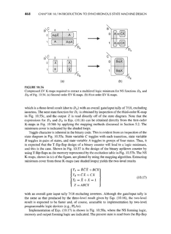
FIGURE 10.56
Compressed EV K-maps required to extract a multilevel logic minimum for NS functions DA and
DB of Fig. 10.54. (a) Second-order EV K-maps. (b) First-order EV K-maps.
which is a three-level result (due to DA) with an overall gate/input tally of 7/18, excluding
inverters. The next state function for DC is obtained by inspection of the third-order K-map
in Fig. 10.55c, and the output Z is read directly off of the state diagram. Note that the
expressions for DA and D B in Eqs. (10.16) can be obtained directly from the first-order
K-maps in Fig. 10.56b by applying the mapping methods discussed in Section 5.2. The
minimum cover is indicated by the shaded loops.
Toggle character is inherent in the binary code. This is evident from an inspection of the
state diagram in Fig. 10.55a. State variable C toggles with each transition, state variable
B toggles in pairs of states, and state variable A toggles in groups of four states. Thus, it
is expected that the T flip-flop design of a binary counter will lead to a logic minimum,
and this is the case. Shown in Fig. 10.57 is the design of the binary up/down counter by
using T flip-flops as the memory represented by the excitation table in Fig. 10.57b. The NS
K-maps, shown in (c) of the figure, are plotted by using the mapping algorithm. Extracting
minimum cover from these K-maps (see shaded loops) yields the two-level results
T A = BCX + BCX
T B=CX + CX
(10.17)
T c = X + X = 1
Z = ABCX
with an overall gate input tally 7/18 excluding inverters. Although the gate/input tally is
the same as that produced by the three-level result given by Eqs. (10.16), the two-level
result is expected to be faster and, of course, amenable to implementation by two-level
programmable logic devices (e.g., PLAs).
Implementation of Eqs. (10.17) is shown in Fig. 10.58a, where the NS forming logic,
memory and output forming logic are indicated. The present state is read from the flip-flop