
Page 499 - Engineering Digital Design
P. 499
State Memory
variable input logic
change value
ABC = Q AQ BQ C
o -+ o 0
0 -> 1
0 ] !> Toggle
1 -»• 1 0
ZiTifX T flip-flop
FSM to be designed Excitation Table
(a) (b)
\BC \BC 01 11 1 \BC 01
A\ oo 01 11 10 A\ °° ° A\ °o 11 10
X o 1 1 1 1
r >l
I J
1 1 1 1
7T C
NS K-maps
(c)
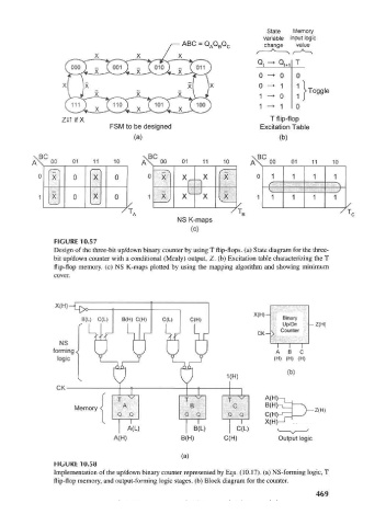
FIGURE 10.57
Design of the three-bit up/down binary counter by using T flip-flops, (a) State diagram for the three-
bit up/down counter with a conditional (Mealy) output, Z. (b) Excitation table characterizing the T
flip-flop memory, (c) NS K-maps plotted by using the mapping algorithm and showing minimum
cover.
NS I I I I ~~l T I
forming ^ \ ) \ ) \ ) \ ) A B C
H
H
H
logic Y . . J L J ( ) ( > ( )
1(H) <b>
Y Y
CK
r 1 r ^ / I T ^ l I T ^ l A H
v >
v /
1r
i r
( )-U_
f I T ^ l
J A A R B n C BfH)-iM x
Memory < •Z(H)
] Q Q Q Q Q Q
k
A(L) B(L) C(L)
A(H) B(H) C(H) Output logic
(a)
FIGURE 10.58
Implementation of the up/down binary counter represented by Eqs. (10.17). (a) NS-forming logic, T
flip-flop memory, and output-forming logic stages, (b) Block diagram for the counter.
469