
Page 496 - Engineering Digital Design
P. 496
466 CHAPTER 10 / INTRODUCTION TO SYNCHRONOUS STATE MACHINE DESIGN
Sampling Interval
x >
\
Proper Improper
Sampling Sampling
(a) (b)
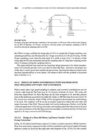
FIGURE 10.54
Examples of proper and improper sampling of the data input, (a) Portion of the resolver state diagram
for an RET D flip-flop, (b) Voltage waveforms showing proper and improper sampling of the D
waveform during the sampling interval of CK.
the FSM is in state a and that the rising edge of CK is to sample the D input waveform, two
sampling possibilities are illustrated by the voltage waveforms for CA'and D in Fig. 10.54b.
Proper sampling occurs when the data input D is stable at logic level 1 in advance of the
rising edge of CK and maintained during the sampling interval. Improper sampling results
when D changes during the sampling interval.
The setup and hold-time intervals are important design parameters for which manufac-
turers will normally provide worst-case data for their flip-flops. Awareness and proper use
of this data is vital to good state machine design practice. Ignoring this data may lead to state
machine unpredictability or even failure. The means to deal with this problem is discussed
later in Section 11.4.
10.12 DESIGN OF SIMPLE SYNCHRONOUS STATE MACHINES WITH
EDGE-TRIGGERED FLIP-FLOPS: MAP CONVERSION
Where nearly ideal, high-speed sampling is required, and economic considerations are not
a factor, edge-triggered flip-flops may be the memory elements of choice. The setup and
hold-time requirements for these flip-flops are the least stringent of all, and they possess
none of the problems associated with either the latches or MS flip-flops discussed earlier. In
this section two relatively simple FSMs will be designed to demonstrate the methodology
to be used. The emphasis will be on the procedure required to obtain the next state and
output functions of the FSM. This procedure will involve nothing new. Rather, it will be the
continued application of the design procedure and mapping algorithm discussed in Section
10.6, and an extension of the flip-flop conversion examples covered in Section 10.8 but now
applied to K-map conversion and FSM design.
10.12.1 Design of a Three-Bit Binary Up/Down Counter: D-to-T
K-map Conversion
In Fig. 10.2d a bidirectional binary sequence of states is used to represent a Mealy machine.
Now, that same binary sequence of states will be completed in the form of a three-bit binary
up/down counter as shown by the eight-state state diagram in Fig. 10.55a. It is this counter