
Page 491 - Engineering Digital Design
P. 491
10.9 LATCHES AND FLIP-FLOPS WITH SERIOUS TIMING PROBLEMS 461
QM(H) QM(H)
D(H) D Q D Q L- Q(H) D(H) D Q D Q -Q(H)
M S M S
CK- Q 3- ry-c > Q D-Q(L) CK — > Q D- -^c CK Q D- Q(L)
r
(a) (b)
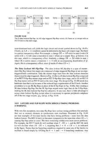
FIGURE 10.48
The D data lockout flip-flop, (a) All edge triggered flip-flop variety, (b) Same as (a) except with an
FET D latch as the slave stage.
reset-dominant basic cell yields the logic circuit and circuit symbol shown in Fig. 10.47e.
Clearly, an S,R — 1,1 condition cannot be delivered to the basic cell output stage. But there
is a partial transparency effect. For example, a change SR -> SR while in state 0 with CK
active (CK =1) will cause a transition to state 1 where Q is issued. Thus, Q follows S in
this case, which is a transparency effect. Similarly, a change SR —> SR while in state 1
when CK is active causes a transition 1 -> 0 with an accompanying deactivation of Q.
Again, this is a transparency effect, since Q tracks R when CK = 1.
The Data Lockout MS Flip-Flop The data lockout MS flip-flop is a type of master-
slave flip-flop whose two stages are composed of edge-triggered flip-flops or are an edge-
triggered/latch combination. Only the master stage must have the data lockout character
(hence must be edge triggered). Shown in Fig. 10.48a is a D data lockout flip-flop composed
of an RET D flip-flop master stage and an FET D flip-flop slave stage, and in (b) an RET D
flip-flop master with an FET D latch as the slave stage. The design in Fig. 10.48b needs less
hardware than that in (a) because of the reduced logic requirements of the D latch. Another
possibility is to use JK flip-flops in place of the D flip-flops in Fig. 10.48a, thus creating a
JK data lockout flip-flop. But the JK flip-flops require more logic than do the D flip-flops,
making the JK data lockout flip-flop less attractive. In any case, there is little advantage to
using a data lockout flip-flop except when it is necessary to operate peripherals antiphase
off of the two stage outputs, Q M and Q, in Fig. 10.48.
10.9 LATCHES AND FLIP-FLOPS WITH SERIOUS TIMING PROBLEMS:
A WARN ING
With very few exceptions, two-state flip-flops have serious timing problems that preclude
their use as memory elements in synchronous state machines. Presented in Fig. 10.49
are four examples of two-state latches that have timing problems — none have the data
lockout feature. The RET D latch (a) becomes transparent to the input data when CK = 1,
causing flip-flop action to cease. The three remaining exhibit even more severe problems.
For example, the FET T latch (b) will oscillate when T • CK = 1, and the RET JK latch
(c) will oscillate when JK • CK = 1, requiring that / = K = CK = 1, as indicated
in the figure. Notice that the branching conditions required to cause any of the latches to
oscillate is found simply by ANDing the 0 -> 1 and 1—^- 0 branching conditions. Any