
Page 506 - Engineering Digital Design
P. 506
476 CHAPTER 10 / INTRODUCTION TO SYNCHRONOUS STATE MACHINE DESIGN
example, if the FSM should power up into don't care state 110 with X inactive (X), it
would transit to state 111 on the next clock triggering edge and would falsely issue an
output Z if X goes active. Ideally, on power-up, this FSM should be initialized into state
000 to properly begin the sequence. Section 11.7 discusses the details by which this can be
accomplished.
10.13 ANALYSIS OF SIMPLE STATE MACHINES
The purpose of analyzing an FSM is to determine its sequential behavior and to identify
any problems it may have. The procedure for FSM analysis is roughly the reverse of the
procedure for FSM design given in Section 10.6. Thus, in a general sense, one begins with
a logic circuit and ends with a state diagram. There are six principal steps in the analysis
process:
1. Given the logic circuit for the FSM to be analyzed, carefully examine it for any
potential problems it may have and note the number and character of its flip-flops, its
inputs, and its outputs (Mealy or Moore).
2. Obtain the NS and output logic functions by carefully reading the logic circuit.
3. Map the output logic expressions into K-maps, and map the NS logic expressions into
K-maps appropriate for the flip-flops used. If the memory elements are other than D
flip-flops, use K-map conversion to obtain D K-maps.
4. From the D K-maps, construct the Present State/Inputs/Next State (PS/NS) table.
To do this, observe which inputs control the branching, as indicated in each cell,
and list these in ascending canonical word form together with the corresponding NS
logic values. Ascending canonical word form means the use of minterm code such as
XYZ, XYZ, XYZ, etc., for branching dependency on inputs X, Y, and Z relative to
a given K-map cell.
5. Use the PS/NS table in step 4 and the output K-maps to construct the fully documented
state diagram for the FSM.
6. Analyze the state diagram for any obvious problems the FSM may have. These
problems may include possible hang (isolated) states, subroutines from which there
are no exits, and timing defects (to be discussed in Chapter 11). Thus, a redesign of
the FSM may be necessary.
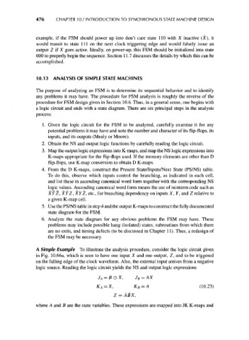
A Simple Example To illustrate the analysis procedure, consider the logic circuit given
in Fig. 10.66a, which is seen to have one input X and one output, Z, and to be triggered
on the falling edge of the clock waveform. Also, the external input arrives from a negative
logic source. Reading the logic circuit yields the NS and output logic expressions
J A = BQX, J B = AX
K A=X, K B = A (10.23)
Z = ABX,
where A and B are the state variables. These expressions are mapped into JK K-maps and