
Page 537 - Engineering Digital Design
P. 537
11.3 DETECTION AND ELIMINATION OF STATIC HAZARDS 507
S(H) J
T(H) J — T(H) J
A H
< ) j I A(H) I
B
(H) J \ B(H) J.
c(H) J ; o/Ln 1
ACT(L) J n ACT(L) J
A§(L) i I i| AS(L) J
Y
SOP(H) J —u CST(L) J
(b)
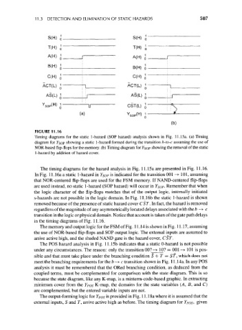
FIGURE 11.16
Timing diagrams for the static 1-hazard (SOP hazard) analysis shown in Fig. 11.15a. (a) Timing
diagram for FSOP showing a static 1-hazard formed during the transition b-to-c assuming the use of
NOR-based flip-flops for the memory, (b) Timing diagram for YSOP showing the removal of the static
1-hazard by addition of hazard cover.
The timing diagrams for the hazard analysis in Fig. 11.15a are presented in Fig. 11.16.
In Fig. 11.16a a static 1-hazard in Y SOp is indicated for the transition 001 -> 101, assuming
that NOR-centered flip-flops are used for the FSM memory. If NAND-centered flip-flops
are used instead, no static 1-hazard (SOP hazard) will occur in Y SOp. Remember that when
the logic character of the flip-flops matches that of the output logic, internally initiated
s-hazards are not possible in the logic domain. In Fig. 11.16b the static 1-hazard is shown
removed because of the presence of static hazard cover CST. In fact, the hazard is removed
regardless of the magnitude of any asymmetrically located delays associated with the b —>• c
transition in the logic or physical domain. Notice that account is taken of the gate path delays
in the timing diagrams of Fig. 11.16.
The memory and output logic for the FSM of Fig. 11.14 is shown in Fig. 11.17, assuming
the use of NOR-based flip-flops and SOP output logic. The external inputs are assumed to
arrive active high, and the shaded NAND gate is the hazard cover, CST.
The POS hazard analysis in Fig. 11.15b indicates that a static 0-hazard is not possible
under any circumstances. The reason: only the transition 00? -» 10? = 001 —>• 101 is pos-
sible and that must take place under the branching condition S + T = ST, which does not
meet the branching requirements for the b —>• c transition shown in Fig. 11.14a. In any POS
analysis it must be remembered that the ORed branching condition, as deduced from the
coupled terms, must be complemented for comparison with the state diagram. This is so
because the state diagram, like any K-map, is a minterm-code-based graphic. In extracting
minimum cover from the Y POs K-map, the domains for the state variables (A, B, and C)
are complemented, but the entered variable inputs are not.
The output-forming logic for Y POs is provided in Fig. 11.18a where it is assumed that the
external inputs, S and T, arrive active high as before. The timing diagram for Y PQS, given