
Page 542 - Engineering Digital Design
P. 542
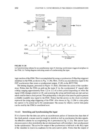
512                 CHAPTER 11 / SYNCHRONOUS FSM DESIGN CONSIDERATIONS


                                         Synchronizer
                                        X        \
                                                    X'(H)   ^
                                          D    Q
                                   nous           Synchronized
                                Input                Input                     Outputs
                                 CK r    )>    Q                  FSM


                                                    (a)

                                          !«-!„„-•!
                              CK _J |_f LJ(^       LJr LJ LJ LJ LJ L_

                              X(H)         | ;      I ;            n
                                                     n             K
                             X'(H)           1
                                                     ,                  \
                                               1 ' FSM '          Narrow data pulse
                                                 CK                  is missed
                                                    (b)
                     FIGURE 11.20
                     (a) Synchronizing scheme for an asynchronous input X showing synchronizer triggered antiphase to
                     the FSM. (b) Timing diagram indicating results of synchronizing the input.


                     logic section of the FSM. This is accomplished by using a synchronizer D flip-flop triggered
                     antiphase to the FSM, as shown in Fig. 11.20a. Here, X(H) is an asynchronous input to the
                     FET synchronizer that issues a synchronized output, X'(H), to the RET FSM.
                       The timing diagram, presented in Figure 11.20(b), illustrates the action of the synchro-
                     nizer. Notice that the FSM can pick up the input X (as the synchronized X' signal) after
                     a delay ranging approximately from 1/2 to 3/2 of a clock period depending on when the
                     signal X(H) changes relative to CK, and assuming the setup and hold times are met and are
                     much smaller than a clock period. This pickup delay is the price that must be paid to present
                     a reliably readable data signal to the FSM. Notice that the arrows on the clock waveform
                     represent the rising edge triggering of the FSM. Also shown in Fig. 11.20b is a data pulse
                     too narrow to be picked up by the synchronizer. The means by which a narrow data pulse
                     can be read by the FSM is considered next.


                     11.4.3 Stretching and Synchronizing the Input
                     If it is known that the data can arrive as asynchronous pulses of duration less than that of
                     the clock period, a means must be sought to stretch as well as synchronize the data signals.
                     An effective scheme for accomplishing this is presented in Fig. 11.2la. The narrow asyn-
                     chronous pulse is first stretched by the set-dominant basic cell (stretcher), then synchronized
                     by the synchronizer. The active low output of the synchronizer is fed back to the R(L) input
                     of the stretcher to reset it in readiness for the next narrow pulse. Notice that the output of