
Page 538 - Engineering Digital Design
P. 538
NOR -based
D A(H) D Q
OX" FFs
A
^
> Q o—
S(H) 1 — ^~ \_
7
T/m y
i \n;
D B(H) — D Q H"^
B
]> Q
°~~
' I>
L
y- y>
Hazard
D C(H) — D Q cover
C
> Q °-
CK
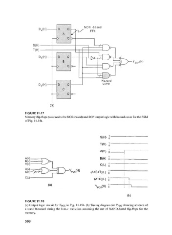
FIGURE 11.17
Memory flip-flops (assumed to be NOR-based) and SOP output logic with hazard cover for the FSM
of Fig. 11.14a.
S(H) ;
A(H) J
B(H) J.
C(L) J
H
POS( ) (A+B+T)(L) J'
(A+§)(L) ;•
POS\ ' 0
(b)
FIGURE 11.18
(a) Output logic circuit for FPQS in Fig. 11.15b. (b) Timing diagram for FPQS showing absence of
a static 0-hazard during the £-to-c transition assuming the use of NAND-based flip-flops for the
memory.
508