
Page 565 - Engineering Digital Design
P. 565
11.9 APPLICATIONS TO THE DESIGN OF MORE COMPLEX STATE MACHINES 535
Use 0 2 = 0 or CK
in P K-map
else (+) glitch
\BC
101 )PiTifCK A\ °° ° 11 10
CK
SfSW.+SWJ 7^~^\ X—^ SW
1
ooo )— ° »( 011 ) ( 111 ) ^> K 001 CK CK
S
PitifCK 'N v
s
v S
A CK + B C
^Y^\ p = ( ) ( K)
(01l)pitifCK \ t \ i
(a) (b)
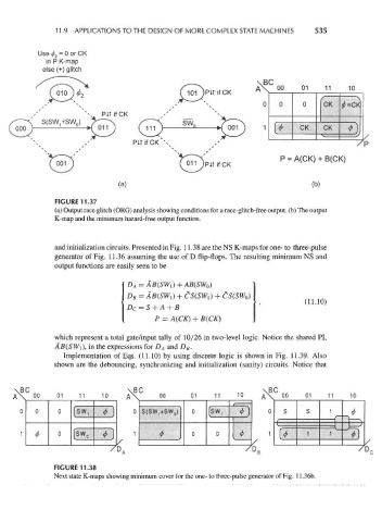
FIGURE 11.37
(a) Output race glitch (ORG) analysis showing conditions for a race-glitch-free output, (b) The output
K-map and the minimum hazard-free output function.
and initialization circuits. Presented in Fig. 11.38 are the NS K-maps for one- to three-pulse
generator of Fig. 11.36 assuming the use of D flip-flops. The resulting minimum NS and
output functions are easily seen to be
(D A = AB(SWi)+AB(SW 0)
= AB(SW {)-i-CS(SW\) + CS(SWo)
D B
(11.10)
DC =S+A+B
P = A(CK) + B(CK)
which represent a total gate/input tally of 10/26 in two-level logic. Notice the shared PI,
AB(S'Wi), in the expressions for D A and D B.
Implementation of Eqs. (11.10) by using discrete logic is shown in Fig. 11.39. Also
shown are the debouncing, synchronizing and initialization (sanity) circuits. Notice that
C \BC \BC
00 01 11 10 A\ 00 01 11 10 A\ °° 01 11 10
o o [sw, ^ ] 0 S(SVW 1 +SW 0 ) 0 [sw, I ] 0 S S 1 (ft
4 =X
1 < . 0 o <l> 1 f^ j 1 <f]
/ f /
FIGURE 11.38
Next state K-maps showing minimum cover for the one- to three-pulse generator of Fig. 11.36b.