
Page 566 - Engineering Digital Design
P. 566
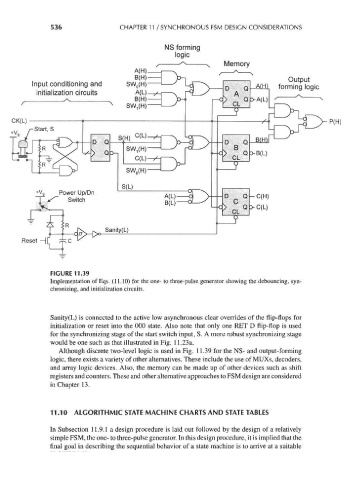
536                 CHAPTER 11 / SYNCHRONOUS FSM DESIGN CONSIDERATIONS


                                                     NS forming
                                                        logic
                                                                      Memory


               Input conditioning and     SW 0(H)   1   ' U~~X         fcI]    Ami formhg togic
                 initialization circuits


                                                                                                    P(H)


                +v s   Power Up/Dn
                ~T~ S~    Switch
                                                                             >C(L)


                    FIGURE 11.39
                    Implementation of Eqs. (11.10) for the one- to three-pulse generator showing the debouncing, syn-
                    chronizing, and initialization circuits.


                    Sanity(L) is connected to the active low asynchronous clear overrides of the flip-flops for
                    initialization or reset into the 000 state. Also note that only one RET D flip-flop is used
                    for the synchronizing stage of the start switch input, S. A more robust synchronizing stage
                    would be one such as that illustrated in Fig. 11.23a.
                      Although discrete two-level logic is used in Fig. 11.39 for the NS- and output-forming
                    logic, there exists a variety of other alternatives. These include the use of MUXs, decoders,
                    and array logic devices. Also, the memory can be made up of other devices such as shift
                    registers and counters. These and other alternative approaches to FSM design are considered
                    in Chapter 13.


                    11.10 ALGORITHMIC STATE MACHINE CHARTS AND STATE TABLES

                    In Subsection 11.9.1 a design procedure is laid out followed by the design of a relatively
                    simple FSM, the one- to three-pulse generator. In this design procedure, it is implied that the
                    final goal in describing the sequential behavior of a state machine is to arrive at a suitable