
Page 560 - Engineering Digital Design
P. 560
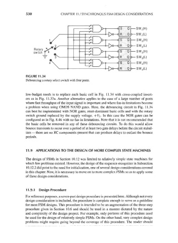
530                 CHAPTER 11 / SYNCHRONOUS FSM DESIGN CONSIDERATIONS


                                                              V-        c S   Q — SW,(H)
                                                        'x
                                                                  — £>o — c R  Q D-SW,(L)
                                                         X
                                                                  i     C S   Q — SW 2(H)
                                                                  -[>o— c R   Q 3— SW 2(L)
                         Rotary                          X    >]
                         switch '*t                                     c S   Q — SW 3(H)
                                                             y>~  4>o— c R    Q >-SW 3 (L)
                                                         S              c S  Q \— SW 4 (H)
                                                        y
                                       >    1                    4>°— < R     Q ^— SW 4 (L)

                     FIGURE 11.34
                     Debouncing a rotary select switch with four posts.


                     low-budget needs is to replace each basic cell in Fig. 11.34 with cross-coupled invert-
                     ers as in Fig. 11.33a. Another alternative applies to the case of a large number of posts
                     where fast throughput of the input signal is important and where fan-in limitations become
                     a problem when using CMOS NAND gates. Here, the debouncing circuit in Fig. 11.34
                     can best be implemented with NOR gates, reset-dominant basic cells and with the rotary
                     switch ground replaced by the supply voltage, +Vs. In this case the NOR gates can be
                     configured as in Fig. 8.46 with no fan-in limitations. Note that it is not recommended that
                     the basic cells be removed in any of these debouncing circuits. To do this would allow
                     bounce transients to occur over a period of at least two gate delays before the circuit stabal-
                     izes — there are no RC components present that can produce delays to outlast the bounce
                     periods.


                     11.9 APPLICATIONS TO THE DESIGN OF MORE COMPLEX STATE MACHINES

                     The design of FSMs in Section 10.12 was limited to relatively simple state machines for
                     which few problems existed. However, the design of the sequence recognizer in Subsection
                     10.12.2 did point to the need for initialization, one of several design considerations covered
                     in this chapter. Now, it is necessary to move on to more complex FSMs so as to apply some
                     of these design considerations.


                     11.9.1 Design Procedure
                     For reference purposes, a seven-part design procedure is presented here. Although not every
                     design consideration is included, the procedure is complete enough to serve as a guideline
                     for most FSM designs. This procedure is intended to be an augmentation of the three-step
                     procedure given in Section 10.6 and should be used in a manner dictated by the nature
                     and complexity of the design project. For example, only portions of this procedure need
                     be used for the design of relatively simple FSMs. On the other hand, very complex design
                     problems might require going beyond the coverage of this procedure. The reader should