
Page 558 - Engineering Digital Design
P. 558
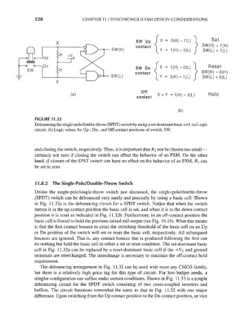
528                 CHAPTER 11 / SYNCHRONOUS FSM DESIGN CONSIDERATIONS


                                                               SW Up      -»     =            Set
                                                              contact S                r SW(H) = 1(H)
                                                    SW(H)              I Y ^ 1(H) = 0(L) I  SW(L) =


                                                               sw Dn J x ^ i(H) = 0(L) 1     Reset
                                                              contact ^                r SW(H) = 0(H)
                                                    SW(L)                Y -» 0(H) = 1(L) I  SW(L) = 0(L)


                                    (a)                        CQc t   X = Y-1(H) = 0(L)    Hold


                                                                                (b)
                     FIGURE 11.32
                     Debouncing the single-pole/double-throw (SPDT) switch by using a set-dominant basic cell, (a) Logic
                     circuit, (b) Logic values for Up-, Dn-, and Off-contact positions of switch, SW.


                     and closing the switch, respectively. Thus, it is important that R 2 not be chosen too small —
                     certainly not zero if closing the switch can affect the behavior of an FSM. On the other
                     hand, if closure of the SPST switch can have no effect on the behavior of an FSM, /?2 can
                     be set to zero.


                     11.8.2 The Single-Pole/Double-Throw Switch
                     Unlike the single-pole/single-throw switch just discussed, the single-pole/double-throw
                     (SPDT) switch can be debounced very easily and precisely by using a basic cell. Shown
                     in Fig. 11.32a is the debouncing circuit for a SPDT switch. Notice that when the switch
                     button is in the up contact position the basic cell is set, and when it is in the down contact
                     position it is reset as indicated in Fig. 11.32b. Furthermore, in an off-contact position the
                     basic cell is forced to hold the previous mixed-rail output (see Fig. 10.16). What this means
                     is that the first contact bounce to cross the switching threshold of the basic cell on an Up
                     or Dn position of the switch will set or reset the basic cell, respectively. All subsequent
                     bounces are ignored. That is, any contact bounce that is produced following the first can
                     do nothing but hold the basic cell in either a set or reset condition. The set-dominant basic
                     cell in Fig. 11.32a can be replaced by a reset-dominant basic cell if the +V$ and ground
                     terminals are interchanged. The interchange is necessary to maintain the off-contact hold
                     requirement.
                       The debouncing arrangement in Fig. 11.32 can be used with most any CMOS family,
                     but there is a relatively high price tag for this type of circuit. For low-budget needs, a
                     simpler configuration can suffice under certain conditions. Shown in Fig. 11.33 is a simple
                     debouncing circuit for the SPDT switch consisting of two cross-coupled inverters and
                     buffers. The circuit functions somewhat the same as that in Fig. 11.32 with one major
                     difference. Upon switching from the Up contact position to the Dn contact position, or vice