
Page 556 - Engineering Digital Design
P. 556
526 CHAPTER 11 / SYNCHRONOUS FSM DESIGN CONSIDERATIONS
/\- '
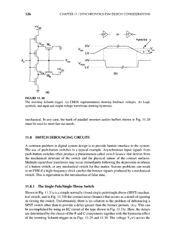
FIGURE 11.30
The inverting Schmitt trigger, (a) CMOS implementation showing feedback voltages, (b) Logic
symbols, and input and output voltage waveforms showing hysteresis.
mechanical. In any case, the bank of parallel inverters and/or buffers shown in Fig. 11.28
must be used to meet fan-out needs.
11.8 SWITCH DEBOUNCING CIRCUITS
A common problem in digital system design is to provide human interface to the system.
The use of push-button switches is a typical example. Asynchronous input signals from
push-button switches often produce a phenomenon called switch bounce that derives from
the mechanical structure of the switch and the physical nature of the contact surfaces.
Multiple open/close transitions may occur immediately following the depression or release
of a button switch, or any mechanical switch for that matter. Serious problems can result
in an FSM if a high-frequency clock catches the bounce signals produced by a mechanical
switch. This is equivalent to the introduction of false data.
11.8.1 The Single-Pole/Single-Throw Switch
Shown in Fig. 11.31 a is a simple normally closed single-pole/single-throw (SPST) mechan-
ical switch, and in Fig. 1 l.Slb the contact noise (bounce) that occurs as a result of opening
or closing the switch. Unfortunately, there is no solution to the problem of debouncing a
SPST switch other than to provide a delay greater than the bounce periods, A? B. This can
be accomplished by using an RC circuit of the type shown in Fig. 11.31 c. Here, the delays
are determined by the choice of the R and C components together with the hysteresis effect
of the inverting Schmitt trigger as in Figs. 11.29 and 11.30. The voltage V x(t) across the