
Page 555 - Engineering Digital Design
P. 555
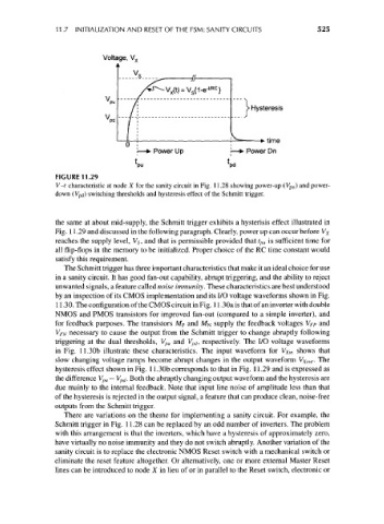
11.7 INITIALIZATION AND RESET OF THE FSM: SANITY CIRCUITS            525


                               Voltage, V


                                                                     Hysteresis


                                                                          time
                                            Power Up            I—*• Power Dn


                  FIGURE 11.29
                  V-t characteristic at node X for the sanity circuit in Fig. 11.28 showing power-up (V pu) and power-
                  down (Vpd) switching thresholds and hysteresis effect of the Schmitt trigger.


                  the same at about mid-supply, the Schmitt trigger exhibits a hysterisis effect illustrated in
                  Fig. 11.29 and discussed in the following paragraph. Clearly, power up can occur before V x
                  reaches the supply level, V s, and that is permissible provided that t pu is sufficient time for
                  all flip-flops in the memory to be initialized. Proper choice of the RC time constant would
                  satisfy this requirement.
                     The Schmitt trigger has three important characteristics that make it an ideal choice for use
                  in a sanity circuit. It has good fan-out capability, abrupt triggering, and the ability to reject
                  unwanted signals, a feature called noise immunity. These characteristics are best understood
                  by an inspection of its CMOS implementation and its I/O voltage waveforms shown in Fig.
                  11.30. The configuration of the CMOS circuit in Fig. 11.30a is that of an inverter with double
                  NMOS and PMOS transistors for improved fan-out (compared to a simple inverter), and
                  for feedback purposes. The transistors M P and M N supply the feedback voltages V FP and
                  VFN necessary to cause the output from the Schmitt trigger to change abruptly following
                  triggering at the dual thresholds, V pu and V pd, respectively. The I/O voltage waveforms
                  in Fig. 11.3Gb illustrate these characteristics. The input waveform for Vx- m shows that
                  slow changing voltage ramps become abrupt changes in the output waveform V Xout- The
                  hysteresis effect shown in Fig. 11.30b corresponds to that in Fig. 11.29 and is expressed as
                  the difference V pu — V pd. Both the abruptly changing output waveform and the hysteresis are
                  due mainly to the internal feedback. Note that input line noise of amplitude less than that
                  of the hysteresis is rejected in the output signal, a feature that can produce clean, noise-free
                  outputs from the Schmitt trigger.
                     There are variations on the theme for implementing a sanity circuit. For example, the
                  Schmitt trigger in Fig. 11.28 can be replaced by an odd number of inverters. The problem
                  with this arrangement is that the inverters, which have a hysteresis of approximately zero,
                  have virtually no noise immunity and they do not switch abruptly. Another variation of the
                  sanity circuit is to replace the electronic NMOS Reset switch with a mechanical switch or
                  eliminate the reset feature altogether. Or alternatively, one or more external Master Reset
                  lines can be introduced to node X in lieu of or in parallel to the Reset switch, electronic or