
Page 559 - Engineering Digital Design
P. 559
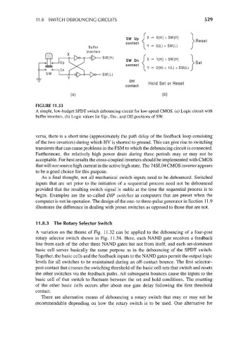
11.8  SWITCH DEBOUNCING CIRCUITS                                     529


                                                        SWU p JX-.0(H)»SW(H )
                                                                Y-»0(L) = SW(L)

                                                        SW Dn J X-* 1(H) = SW(H)  I   {


                                                        contact  Hold Set  ° r R6S6t
                                 (a)                                  (b)

                  FIGURE 11.33
                  A simple, low-budget SPDT switch debouncing circuit for low-speed CMOS, (a) Logic circuit with
                  buffer inverters, (b) Logic values for Up-, Dn-, and Off-positions of SW.


                  versa, there is a short time (approximately the path delay of the feedback loop consisting
                  of the two inverters) during which HV is shorted to ground. This can give rise to switching
                  transients that can cause problems in the FSM to which the debouncing circuit is connected.
                  Furthermore, the relatively high power drain during these periods may or may not be
                  acceptable. For best results the cross-coupled inverters should be implemented with CMOS
                  that will not source high current in the active high state. The 74SL04 CMOS inverter appears
                  to be a good choice for this purpose.
                     As a final thought, not all mechanical switch inputs need to be debounced. Switched
                  inputs that are set prior to the initiation of a sequential process need not be debounced
                  provided that the resulting switch signal is stable at the time the sequential process is to
                  begin. Examples are the so-called DIP switches in computers that are preset when the
                  computer is not in operation. The design of the one- to three-pulse generator in Section 11.9
                  illustrates the difference in dealing with preset switches as opposed to those that are not.


                  11.8.3 The Rotary Selector Switch

                  A variation on the theme of Fig. 11.32 can be applied to the debouncing of a four-post
                  rotary selector switch shown in Fig. 11.34. Here, each NAND gate receives a feedback
                  line from each of the other three NAND gates but not from itself, and each set-dominant
                  basic cell serves basically the same purpose as in the debouncing of the SPDT switch.
                  Together, the basic cells and the feedback inputs to the NAND gates permit the output logic
                  levels for all switches to be maintained during an off-contact bounce. The first selector-
                  post contact that crosses the switching threshold of the basic cell sets that switch and resets
                  the other switches via the feedback paths. All subsequent bounces cause the inputs to the
                  basic cell of that switch to fluctuate between the set and hold conditions. The resetting
                  of the other basic cells occurs after about one gate delay following the first threshold
                  contact.
                    There are alternative means of debouncing a rotary switch that may or may not be
                  recommendable depending on how the rotary switch is to be used. One alternative for