
Page 552 - Engineering Digital Design
P. 552
522 CHAPTER 1 1 / SYNCHRONOUS FSM DESIGN CONSIDERATIONS
Sampling Intervals
CK / \ S
D I \ |
Q . y r
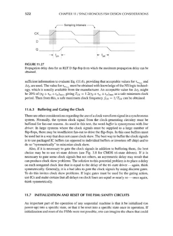
FIGURE 11.27
Propagation delay data for an RET D flip-flop from which the maximum propagation delay can be
obtained.
sufficient information to evaluate Eq. (11.6), providing that acceptable values for r M5max and
Afyj are used. The value for r n?max must be obtained with knowledge of the NS logic technol-
ogy, which is usually available from the manufacturer. An acceptable value for Af/j might
be 20% of (iff + r ns + t su) max, giving T CK = 1 -2(r ff + r ns + t su) max as a safe minimum clock
period. Then from this, a safe maximum clock frequency fcK = 1 / TCK can be obtained.
11.6.3 Buffering and Gating the Clock
There are other considerations regarding the use of a clock waveform signal in a synchronous
system. Normally, the system clock signal from the clock-generating circuitry must be
buffered for fan-out reasons. As used in this text, the word buffer is synonymous with line
driver. In large systems where the clock signals must be supplied to a large number of
flip-flops, there may be insufficient fan-out to drive the flip-flops. In this case buffers must
be used but in a way that does not cause clock skew. The best way to buffer the clock signals
is to use packaged 1C buffers (as opposed to individual buffers or inverters off chip) and to
do so "symmetrically" to minimize clock skew.
Also, if it is necessary to gate the clock signals in addition to buffering them, the best
choice may be to use tri-state drivers (see Fig. 3.8 for CMOS tri-state drivers). If it is
necessary to gate some clock signals but not others, an asymmetric delay may result that
can produce clock skew problems. The solution to this potential problem is to place a delay
on each nongated clock line that is equal to the delay of the tri-state driver — again, think
symmetrically. Generally, it is a bad idea to gate the clock signals by using discrete gates.
To do this invites clock skew problems. If logic gates must be used for the gating action,
use ICs and make certain that all delays on clock lines are equal or nearly so — once again,
think symmetrically.
11.7 INITIALIZATION AND RESET OF THE FSM: SANITY CIRCUITS
An important part of the operation of any sequential machine is that it be initialized (on
power-up) into a specific state, or that it be reset into a specific state once in operation. If
initialization and reset of the FSMs were not possible, one can imagine the chaos that could