
Page 548 - Engineering Digital Design
P. 548
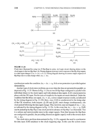
518                CHAPTER 11 /SYNCHRONOUS FSM DESIGN CONSIDERATIONS


                                                        _^(H)               Q 2(H)
                                      X(H)       D    Q           D     Q

                                            r   >CK, Q  r |—      >o<2 Q  o—
                                           At,              At 2


                                      \(
                                                           (a)


                          X(H)
                         Q,(H)
                         Q 2(H)


                                     At 2 = At, = 0                         At 2 > At,
                                         (b)                                   (c)
                     FIGURE 11.24
                    Clock skew illustrated by using two D flip-flops in series, (a) Logic circuit showing delays on the
                    clock inputs to the two flip-flops, (b) Timing diagram showing correct response of the flip-flop outputs
                    to a data input change if A?i = A?2 = 0. (c) Timing diagram showing erroneous output response of
                    flip-flops due to a data change when A?2 > Af i.


                     synchronizer under the condition A?2 — A?] > Tff, little or no protection is provided against
                    metastability.
                       Another type of clock skew problem can occur when the data are presented in parallel, as
                    depicted in Fig. 11.25. Shown in Fig. 11.25a are two D flip-flops configured in parallel with
                    individual delays to the clock inputs and with identical data inputs X(H) synchronized in
                    phase with the CK input. For the sake of simplicity the inputs are made identical. Under the
                    condition that the delays are equal, A?2 = A?i, correct output response results, as indicated
                    by the timing diagram in Fig. 11.25b. Here, since X(H) is synchronized to the rising edge
                    of the CK waveform, both outputs, Q\(H) and Q2(H), must change simultaneously, one
                    clock period following the data input change. This, however, may not happen if Ar 2 > Ati,
                    as indicated by the timing diagram in Fig. 11.25c. In the event that A?2 — Af] > Tff, X(H)
                    can be picked up by flip-flop 2 one clock period in advance of flip-flop 1 as illustrated. This
                    is a serious and unrecoverable error in the output signals. Note that because the flip-flops
                    are configured in parallel, the preceding discussion applies equally well to the reverse skew
                     A?i > A? 2-
                       The clock skew problem demonstrated in Fig. 11.25c supports the need to synchronize
                    the data input X(H) antiphase to the clock triggering edge. In this case the system issues