
Page 549 - Engineering Digital Design
P. 549
11.5 CLOCK SKEW 519
1
CK
At, X (H) At, X (H)
1 1
1 1
E)
CKa °
Q Q Q Q
(a)
CK 1 = CK 2 =
X(H)
Q 2(H).
At 2 = At 1 = 0
(b)
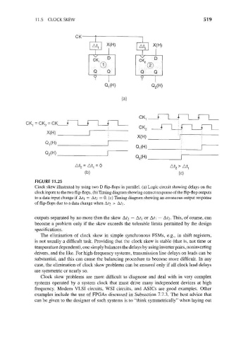
FIGURE 11.25
Clock skew illustrated by using two D flip-flops in parallel, (a) Logic circuit showing delays on the
clock inputs to the two flip-flops, (b) Timing diagram showing correct response of the flip-flop outputs
to a data input change if Af i = A?2 = 0. (c) Timing diagram showing an erroneous output response
of flip-flops due to a data change when A/2 > A/i.
outputs separated by no more than the skew A? 2 — A?i or A?i — Ar 2- This, of course, can
become a problem only if the skew exceeds the tolerable limits permitted by the design
specifications.
The elimination of clock skew in simple synchronous FSMs, e.g., in shift registers,
is not usually a difficult task. Providing that the clock skew is stable (that is, not time or
temperature dependent), one simply balances the delays by using inverter pairs, noninverting
drivers, and the like. For high-frequency systems, transmission line delays on leads can be
substantial, and this can cause the balancing procedure to become more difficult. In any
case, the elimination of clock skew problems can be ensured only if all clock lead delays
are symmetric or nearly so.
Clock skew problems are more difficult to diagnose and deal with in very complex
systems operated by a system clock that must drive many independent devices at high
frequency. Modern VLSI circuits, WSI circuits, and ASICs are good examples. Other
examples include the use of FPGAs discussed in Subsection 7.7.3. The best advice that
can be given to the designer of such systems is to "think symmetrically" when laying out