
Page 592 - Engineering Digital Design
P. 592
562 CHAPTER 12 / MODULE AND BIT-SLICE DEVICES
independent of its input logic status is called true hold. The most complex shift register and
one that is designed to operate in all four modes just listed is called the universal shift register.
These and other shift registers will be considered in some detail during the discussions that
follow. Here, the modular approach to register design is emphasized, featuring the design
of a 1-bit slice, the 7th stage, which can be cascaded to form a register of any size. After
completing this section, the reader will be familiar with most any shift register available
commercially.
Registers are used in a wide variety of digital systems. They are used in the temporary
storage of binary data, in data transmission, in arithmetic operations, in counter design, in
accumulators, and in a host of other specialized applications. Registers are even used as
memory elements in FSM design.
12.2.1 The Storage (Holding) Register
A register whose only function is to store information is called a storage register and is some-
times referred to as a parallel-in/parallel-out or PIPO register. It is, of course, the simplest
of all registers, since it consists of nothing more than an array of synchronously triggered
D flip-flops with independent data inputs. Shown in Figs. 12.1a and 12. Ib are the state
diagram and NS K-map for the /th stage of a storage register. Notice that the NS function
Dj obtained from the K-map is trivial since it can be easily deduced from the state diagram.
Storage (holding) registers are commonly used in the output stage of FSMs to filter out
logic noise. A one-bit holding register is featured in Fig. 11.7, where it is used to filter the
logic noise in output Z from the FSM. Storage registers are also used to provide ordered
delivery of parallel data. For example, combinational adders, subtracters, multipliers, di-
viders, and arithmetic logic units all require the data to be introduced in an ordered and
parallel fashion, an operation that is easily accomplished by using storage registers. A four-
bit adder/subtractor of the type shown in Fig. 8.9 would require two four-bit PIPO registers,
one for word A and the other for word B. The sums may also require such a register.
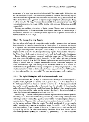
12.2.2 The Right Shift Register with Synchronous Parallel Load
The operation table for the /th stage of a unidirectional shift register that can operate in
only two modes, right shift and parallel load, is given in Fig. 12.2a. It is the function of
this shift register that when the mode control S is inactive (S = 0) the register must shift
right one bit on each triggering edge of clock, and when S is active (S = 1) it must parallel
load synchronously. Synchronous parallel load means that the load values appearing on the
input to the register will be loaded into the register's flip-flops by the action of clock, not
via the flip-flop's asynchronous preset and clear overrides.
Shown in Fig. 12.2b is the state diagram for the shift register as derived from the operation
table in Fig. 12.2a. Notice that the branching condition f ab is obtained by ANDing the mode
control logic (in the S column of the operation table) with the corresponding next state action
parameter (in the NSj column) for each operation that can introduce a set condition (0 —>• 1)
into the register, and then ORing the results. Thus, both a right shift Qj+\ or a parallel
load Pj operation can produce a set condition, hence f ab = SQ J+l + SPj. The set hold
branching condition, fc, must contain all that is in f ah, hence f b = f ab, as is true for the D
flip-flop in Fig. 10.23b. The other two branching conditions follow from the sum rule but
need not be specified in plotting the K-map for Dj, given in Fig. 12.2c. The NS logic for