Page 597 - Engineering Digital Design
P. 597

12.2  REGISTERS                                                      567


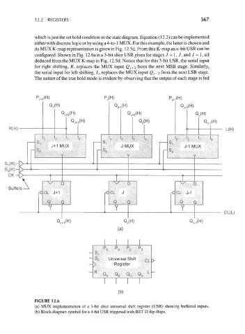
                 which is just the set hold condition in the state diagram. Equation (12.2) can be implemented
                 either with discrete logic or by using a 4-to-1 MUX. For this example, the latter is chosen and
                 its MUX K-map representation is given in Fig. 12.5d. From this K-map an n-bit USR can be
                 configured. Shown in Fig. 12.6a is a 3-bit slice USR given for stages J + l, J, and J — 1, all
                 deduced from the MUX K-map in Fig. 12.5d. Notice that for this 3-bit USR, the serial input
                 for right shifting, R, replaces the MUX input Qj+2 from the next MSB stage. Similarly,
                 the serial input for left shifting, L, replaces the MUX input Qj-i from the next LSB stage.
                 The nature of the true hold mode is evident by observing that the output of each stage is fed


                   P i(H)                      Pj(H)                     Pj.^H)
                    J+
                        Qj(H)                      Qj-i(H)                    Qj. 2(H)
                             QJ <-2\ H)                 QJ+1 H)                     Qj(H)
                                 Qj*i(H)                     Qj(H)                     Qj-i(H)
        R(H)                   •                                                ••              L(H)
                           '
                      a         1   n            3    ?    1   ft           3    2   1    0
                   S.                         S.                         S.
                         J+1 MUX                      JMUX                     J-1 M\JX
                   S                          c                          S
                                               0
                    °        Y                          Y                          Y
        ,u\  i[x  ,
       1
            X,
       CK-  X                                       I                         !
             *          \/   D                     x/   D                     v D
        Buffers — ^
                    -C CL  J+1                 rC CL  J                   rC CL  J-1
                        Q    Q                     Q    Q                     Q    Q
                        Y                          Y                          Y
                                                                                                OL^L;
                                               •                                                n (\ }
                                                       Qj(H)                      Qj.^H)
                                                    (a)


                                              P    P    P    P
                                              r
                                               A   r B   C   D
                                           S 0   Universal Shift
                                           >       Register
                                           R  /~s  i~\  r\


                                                    (b)
                 FIGURE 12.6
                 (a) MUX implementation of a 3-bit slice universal shift register (USR) showing buffered inputs.
                 (b) Block diagram symbol for a 4-bit USR triggered with RET D flip-flops.
   592   593   594   595   596   597   598   599   600   601   602