
Page 598 - Engineering Digital Design
P. 598
568 CHAPTER 12 / MODULE AND BIT-SLICE DEVICES
Parallel load in, PI
Buffers PA PB PC PD PE Pp PG PH
/
CK
P
A PB PC PO
S 1
Universal Shift 1 Universal Shift
S 0 b-
Register )> Register
SI for Rgt. shift =R(H)- R -L(H) = SI for Lft. shift
QA QB Q c Q A Q 8 Q c Q D
SO for Lft. shift SO for Rgt. shift
Q Q
c QD QE QF QG H
Parallel load out, PO
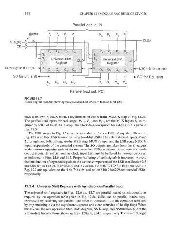
FIGURE 12.7
Block diagram symbols showing two cascaded 4-bit USRs to form an 8-bit USR.
back to its own 7 0 MUX input, a requirement of cell 0 in the MUX K-map of Fig. 12.5d.
The parallel load inputs for each stage, P y+) , P/, and P/_i are the MUX inputs 7 3, as re-
quired by cell 3 of the MUX K-map. The block diagram symbol for a 4-bit USR is given in
Fig. 12.6b.
The USR stages in Fig. 12.6 can be cascaded to form a USR of any size. Shown in
Fig. 12.7 is an 8-bit USR formed by using two 4-bit USRs. The external serial inputs, R and
L, for right and left shifting, are the MSB stage MUX 7) input and the LSB stage MUX 7 2
input, respectively, of the cascaded system. The SO outputs are taken from the Q outputs
at the extreme opposite ends of the two cascaded USRs as shown. Also, note that mode
control inputs, S\ and So, and the clock input CK must be buffered for fan-out purposes,
as indicated in Figs. 12.6 and 12.7. Proper buffering of such signals is important to avoid
the introduction of degraded signals to the various components of the USR (see Section 3.5
and Subsection 11.6.3). Individually and in cascade, but with FET D flip-flops, the USRs in
Fig. 12.7 are equivalent to the 4-bit 74xxl94 and to the 8-bit 74xx299 commercial USRs,
respectively.
12.2.4 Universal Shift Registers with Asynchronous Parallel Load
The universal shift registers in Figs. 12.6 and 12.7 are parallel loaded synchronously as
required by the operation table given in Fig. 12.5a. USRs can be parallel loaded asyn-
chronously by removing the parallel load mode of operation from the operation table and
by implementing it via the asynchronous preset and clear overrides of the flip-flops. When
this is done, the new operation table, state diagram, NS K-map, and NS function Dj for the
yth module become those shown in Figs. 12.8a, b, and c, respectively. The resulting logic